Plasma processing apparatus and method for plasma-processing semiconductor substrate

a processing apparatus and semiconductor substrate technology, applied in the direction of plasma technique, chemical vapor deposition coating, coating, etc., can solve the problems of increasing the charge-up damage of the semiconductor substrate, the damage of the mos transistor, etc., to reduce the amount of plasma generated, increase the processing efficiency, and reduce the effect of stopping the generation of plasma

Inactive Publication Date: 2010-11-04
TOKYO ELECTRON LTD
View PDF6 Cites 216 Cited by
  • Summary
  • Abstract
  • Description
  • Claims
  • Application Information

AI Technical Summary

Benefits of technology

[0016]In other words, according to the plasma processing apparatus and the method for plasma-processing a semiconductor substrate, the plasma processing efficiency can be increased by arranging a semiconductor substrate in a first region having a high electron temperature of plasma during a

Problems solved by technology

Here, when the plasma process is performed on a semiconductor substrate by using the each plasma, electric charges are accumulated in a gate oxide film (gate insulation film) or an adjacent layer included in a MOS transistor, and thus the MOS transistor has plasma damage, such as charge-up.
How

Method used


Image

  • Plasma processing apparatus and method for plasma-processing semiconductor substrate
  • Plasma processing apparatus and method for plasma-processing semiconductor substrate
  • Plasma processing apparatus and method for plasma-processing semiconductor substrate

Examples


Embodiment Construction

Best Mode for Carrying Out the Invention

[0027]Hereinafter, embodiments of the present invention will be described in detail with reference to the attached drawings.

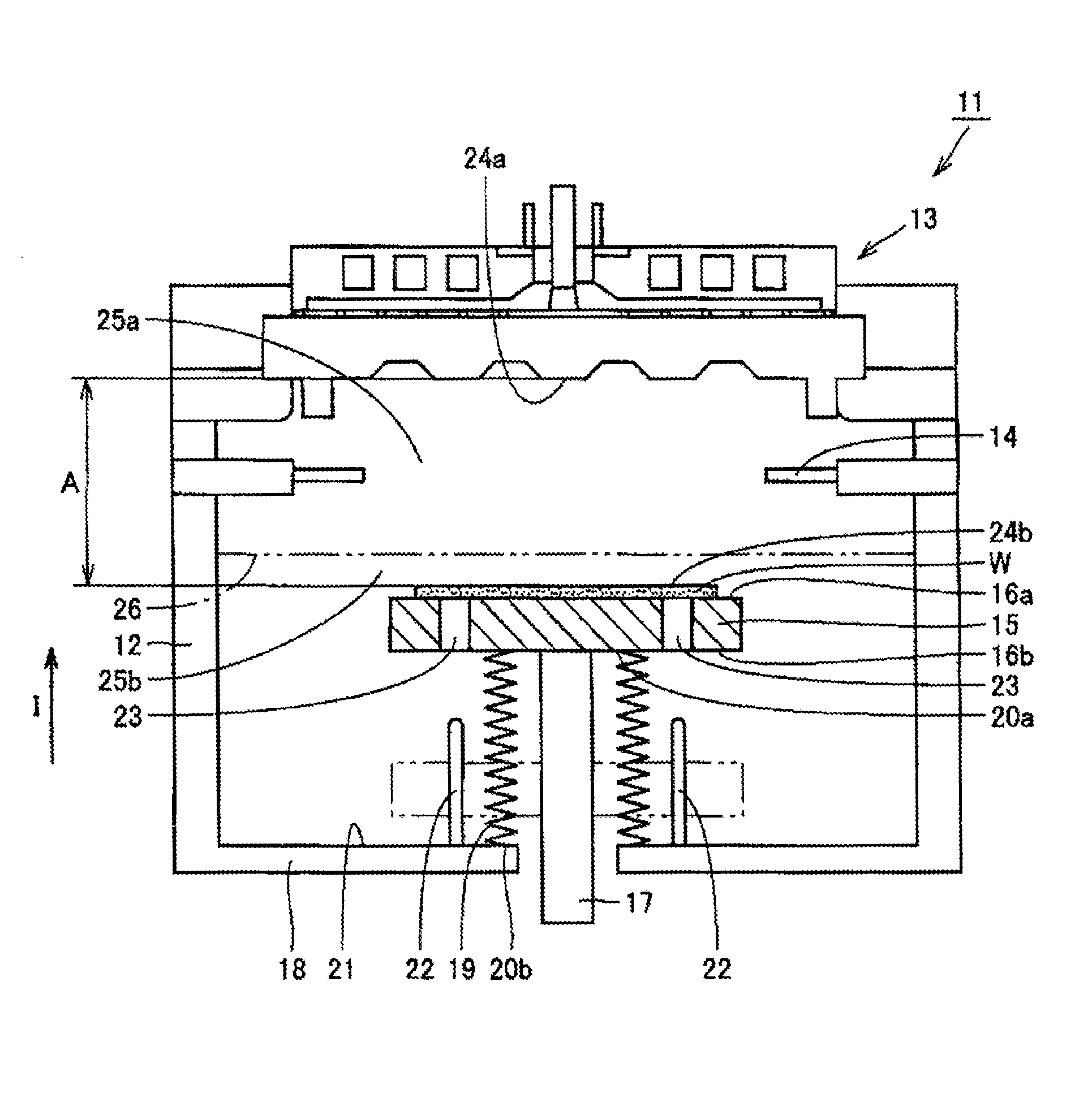
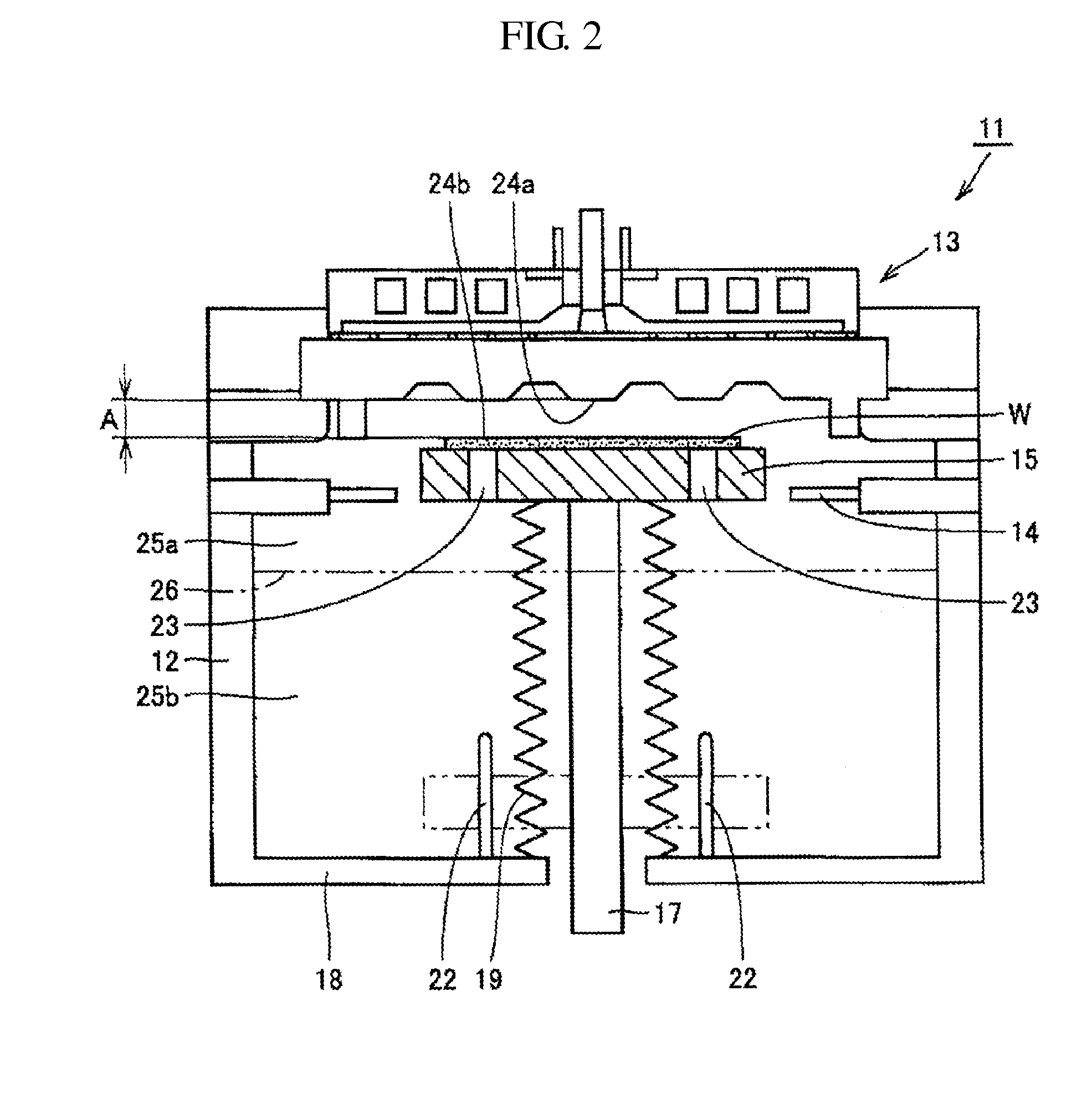
[0028]FIG. 1 is a cross-sectional view schematically showing a part of a plasma processing apparatus according to an embodiment of the present invention. Also, in the following drawings, the top of a paper on which a drawing is drawn is assumed to be an upper direction. Furthermore, a semiconductor substrate W to be processed may include a MOS transistor.

[0029]Referring to FIG. 1, a plasma processing apparatus 11 includes a sealable chamber (container) 12 for performing a plasma process on the semiconductor substrate W to be processed, by accommodating the semiconductor substrate W, an antenna unit 13 serving as a plasma generating means for generating plasma in the chamber 12 by using microwaves fed from a waveguide, and a gas inlet 14 serving as an inlet path of an etching gas into the chamber 12.

[0030]A holding stage 1...


PUM

PropertyMeasurementUnit
Energyaaaaaaaaaa
Pressureaaaaaaaaaa
Electron temperatureaaaaaaaaaa

Abstract

A plasma processing apparatus includes an antenna unit for generating plasma by using microwaves as a plasma source in such a way that a first region having a relatively high electron temperature of plasma, and a second region having a lower electron temperature of plasma than the first region are formed in a chamber, a first arranging means for arranging a semiconductor substrate W in the first region, a second arranging means for arranging the semiconductor substrate in the second region, and a plasma generation stopping means for stopping the generation of plasma of a plasma generating means, while the semiconductor substrate is arranged in the second region.

Description

TECHNICAL FIELD[0001]The present invention relates to a plasma processing apparatus and a method for plasma-processing a semiconductor substrate, and more particularly, to a plasma processing apparatus for performing an etching process or a CVD process by using plasma, and a method for plasma-processing a semiconductor substrate.BACKGROUND ART[0002]Semiconductor devices, such as LSI (Large Scale Integrated circuit), are manufactured via a plurality of processes, such as etching, CVD (Chemical Vapor Deposition), and sputtering, performed with respect to a semiconductor substrate (wafer). These processes, such as etching, CVD, and sputtering, may use plasma as an energy supply source, that is, may be plasma etching, plasma CVD, and plasma sputtering.[0003]When manufacturing a semiconductor device, the plasma processes described above are effectively used along with the recent miniaturization or multilayered-wiring of LSI. For example, when performing a plasma process for manufacturing...

Claims


Application Information

Patent Timeline
IPC IPC(8): H01L21/465H01L21/46
CPCC23C16/511C23C16/52H05H1/46H01J37/32266H01J37/32954H01J37/32192
Inventor UDEA, HIROKAZUNISHIZUKA, TETSUYANOZAWA, TOSHIHISAMATSUOKA, TAKAAKI
Owner TOKYO ELECTRON LTD
Why Eureka
Try Eureka