Bonding wire for semiconductor device

Active Publication Date: 2010-11-11
NIPPON MICROMETAL CO LTD +1
View PDF5 Cites 24 Cited by
  • Summary
  • Abstract
  • Description
  • Claims
  • Application Information

AI Technical Summary

Benefits of technology

[0041]With the bonding wire for a semiconductor device according to the present invention, wire leaning at the upright portion of a ball (leaning failure) can be improved. Moreover, spring failure which becomes a problem in stacked chip bonding or the like can be suppressed. Loop linearity and loop height s

Problems solved by technology

Loop shape has become complex due to the density growth in the semiconductor packaging technologies.
On the other hand, bad influences, such as bondability degradation and increase in electrical resistance may occur due to such alloying, and therefore, it is difficult to comprehensively satisfy the various properties required for a bonding wire.
With a bonding wire made of copper, however, there are problem

Method used


Image

  • Bonding wire for semiconductor device
  • Bonding wire for semiconductor device
  • Bonding wire for semiconductor device

Examples


Example

Examples

[0098]Examples will be explained below.

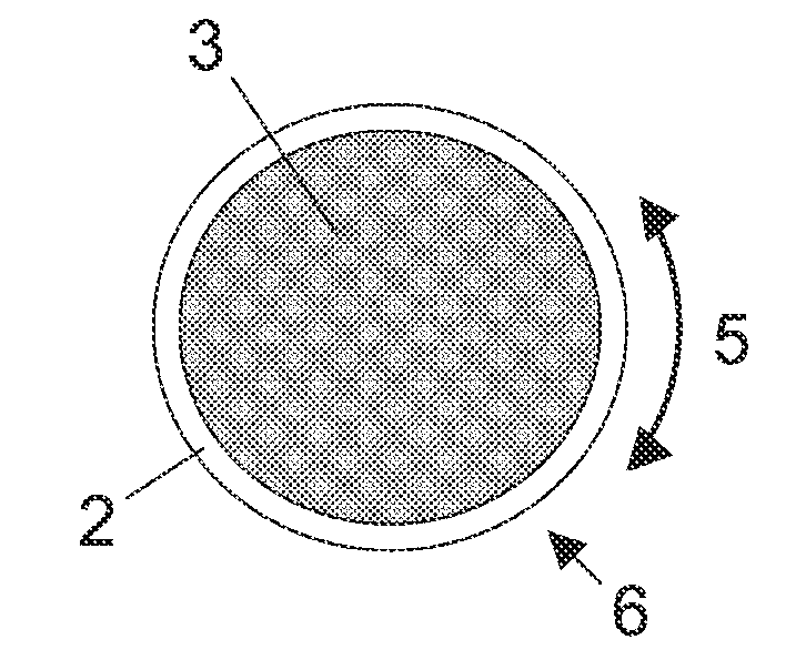
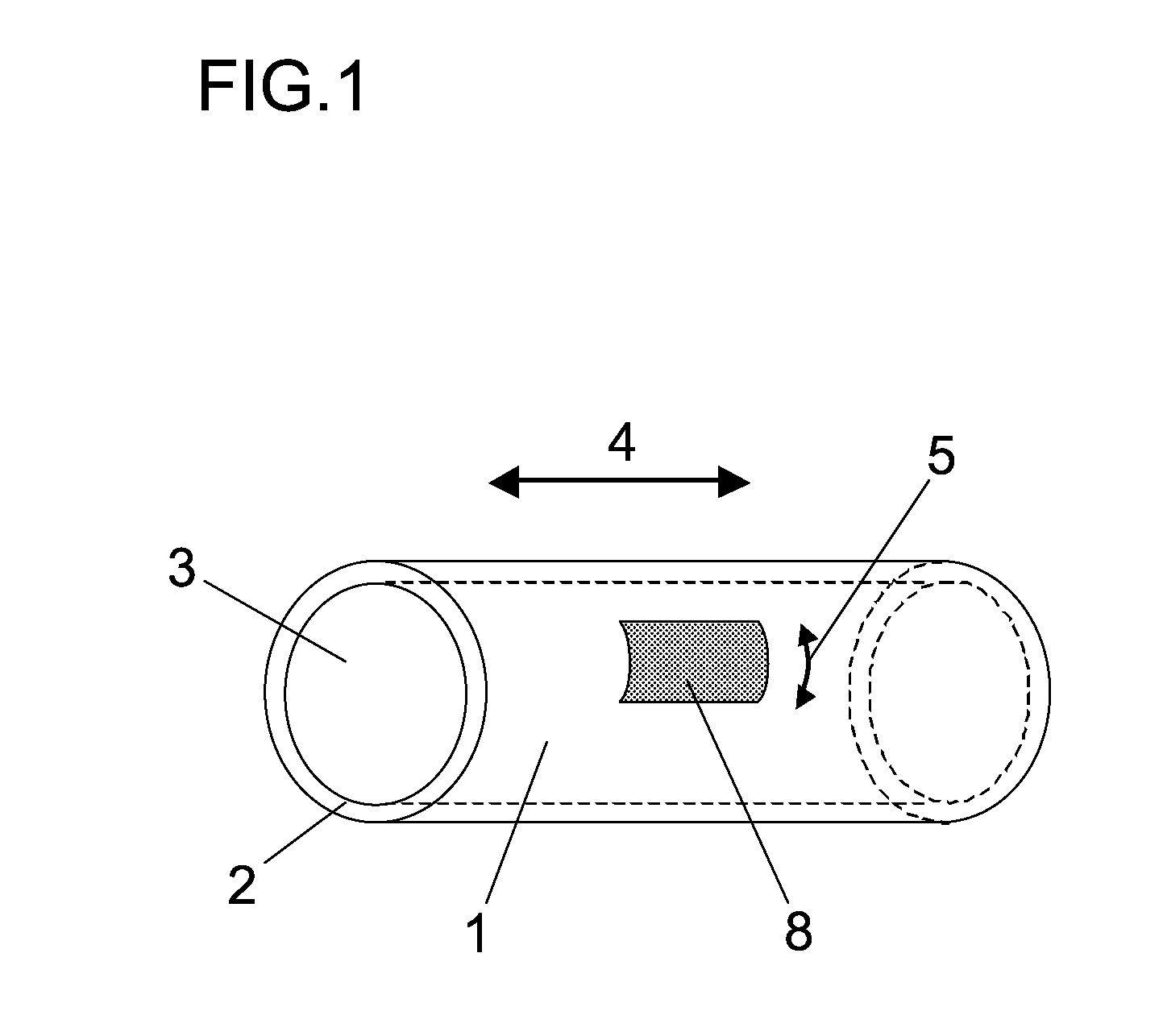
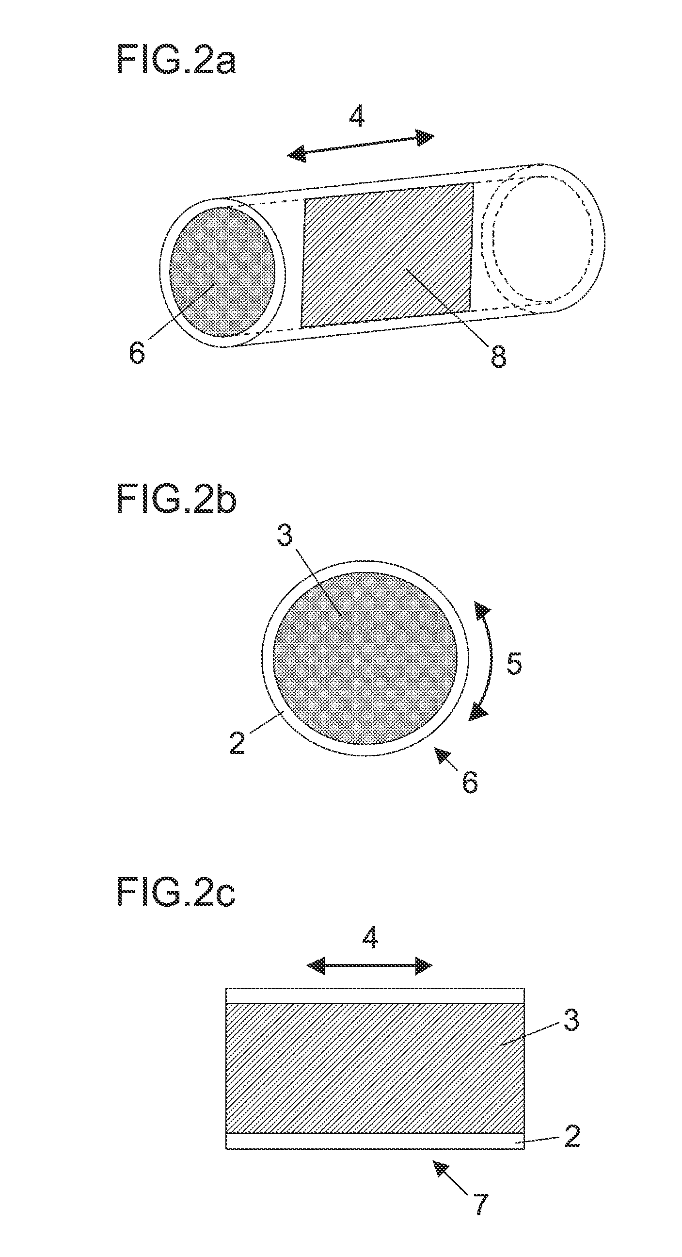
[0099]Regarding the raw materials for a bonding wire, high-purity materials for Cu, Au, and Ag with a purity of approximately 99.99% by mass or greater were used for the core material, and materials of Au, Pt, Pd, Ru, Rh, and Ag with a purity of 99.9% by mass or greater were used for the skin layer or the intermediate metal layer.

[0100]To use a thinned wire to a certain diameter as the core material and to form a layer of a different metal on the surface of the wire, an electroplating, electroless plating, evaporation, or melting method was carried out and then, heat treatment was performed. As the electroplating solution and electroless plating solution, commercially available plating solutions for semiconductor technologies were used, and sputtering was used as the evaporation method. A wire having a diameter of approximately 25 to 1500 μm was prepared in advance and a coating was applied on the surface of the wire by evaporation, pl...

Example

[0138]A multilayer-structured bonding wire corresponding to the examples 2, 8, 9, 25, 27, and 34 to 36, which is in accordance with the present invention, comprises Cu as the main component constituting the core material, and the core material contains one or more of In, Ca, B, Pd, Bi, Zr, Ag, and P in a range of 5 to 300 ppm. For this reason, it was confirmed that the linearity at short span and low loop was improved. Similarly, the examples 19, 20, 22, and 30 to 32, which are in accordance with the present invention, comprise Au as the main component constituting the core material, and the core material contains at least one of Be, Ca, Ni, Pd, and Pt in a range of 5 to 9500 ppm. For this reason, it was confirmed that the linearity at short span and low loop was improved.

Example

[0139]A multilayer-structured bonding wire corresponding to the examples 12, and 36 to 40, which is in accordance with the present invention, comprises Cu as the main component constituting the core material and Pd or Ag as the main component of the skin layer, and contains Pd in a range of 5 to 10000 ppm. For this reason, it was confirmed that the bending property at overhang type stacked chip reverse bonding was improved. Preferably, with the examples 12, and 37 to 40, since the Pd concentration was in the range of 200 to 10000 ppm, a high effect of improving the bump height at overhang type stacked chip reverse bonding was confirmed. Moreover, since the Pd concentration was in the range of 5 to 8000 ppm in the examples 12, 36 to 38, and 40, it was confirmed that chip damage was suppressed. On the other hand, since the Pd concentration exceeded 8000 ppm in the example 39, it was confirmed that chip damage increased.

[0140]The examples 41 to 80 shown in Table 3 correspond to bonding...


PUM

PropertyMeasurementUnit
Fractionaaaaaaaaaa
Fractionaaaaaaaaaa
Fractionaaaaaaaaaa

Abstract

An object of the present invention is to provide a high-performance bonding wire that is suitable for semiconductor mounting technology, such as stacked chip bonding, thinning, and fine pitch mounting, where wire lean (leaning) at an upright position of a ball and spring failure can be suppressed and loop linearity and loop height stability are excellent. This bonding wire for a semiconductor device includes a core material made of a conductive metal, and a skin layer formed on the core material and containing a metal different from the core material as a main component; wherein a relationship between an average size (a) of crystal grains in the skin layer on a wire surface along a wire circumferential direction and an average size (b) of crystal grains in the core material on a normal cross section, the normal cross section being a cross section normal to a wire axis, satisfies an inequality of a/b≦0.7.

Description

TECHNICAL FIELD[0001]The present invention relates to a bonding wire for a semiconductor device to be used for connection between an electrode on a semiconductor element and a wiring line of a circuit wiring substrate (e.g., a lead frame, a substrate, a tape, and so on).BACKGROUND ART[0002]At present, thin wires (bonding wires) having a diameter of approximately 20 to 50 μm are being mainly used as bonding wires for connection between the electrodes on a semiconductor element and external terminals. To bond a bonding wire, thermocompression bonding with the aid of ultrasound is commonly used, where a general-purpose bonding apparatus, a capillary jig into which a bonding wire is inserted for connection, or the like, is used. The tip of a bonding wire is heated and melted by arc heat input, thereby forming a ball by surface tension. Then the ball portion thus formed is compressively bonded onto an electrode of a semiconductor element that has been heated in a range of 150 to 300° C.,...

Claims


Application Information

Patent Timeline
IPC IPC(8): H01B5/00
CPCH01L2224/45139H01L2224/45572H01L2224/45673H01L2224/48247H01L2224/48471H01L2224/4848H01L2224/48511H01L2224/85065H01L2224/85207H01L2224/85444H01L2924/01024H01L2924/01044H01L2924/01045H01L2924/15747H01L2225/06562H01L2924/01327H01L2224/48624H01L2224/48227H01L2224/48479H01L2224/85186H01L2924/00015H01L2924/12041B21C37/047B23K35/0261B23K35/0272B23K35/24B23K35/30B23K35/3006B23K35/3013B23K35/302C22C5/02C22C9/00C22F1/08C22F1/14H01L24/43H01L24/45H01L24/85H01L2224/05624H01L2224/4312H01L2224/4321H01L2224/45015H01L2224/45144H01L2224/45147H01L2224/45565H01L2224/456H01L2224/45639H01L2224/45644H01L2224/45664H01L2224/45669H01L2224/45676H01L2224/4851H01L2224/85045H01L2224/85075H01L2224/85439H01L2924/01004H01L2924/01005H01L2924/01006H01L2924/01007H01L2924/01013H01L2924/01014H01L2924/01015H01L2924/01018H01L2924/0102H01L2924/01022H01L2924/01025H01L2924/01027H01L2924/01028H01L2924/01029H01L2924/01033H01L2924/0104H01L2924/01046H01L2924/01047H01L2924/01049H01L2924/01078H01L2924/01079H01L2924/01082H01L2924/01083H01L2924/10253H01L2924/14H01L2924/20752H01L2924/3025H01L2224/48011H01L2224/4849H01L2224/43825H01L2224/43848H01L2224/43986H01L2924/01203H01L2224/45655H01L2224/45657H01L2224/45671H01L2224/45666H01L2924/20105H01L2924/20106H01L2924/20107H01L2924/01204H01L2924/01202H01L2224/48465H01L2924/20751H01L2924/01001H01L2924/20655H01L2924/20652H01L2924/20653H01L2924/20654H01L2924/20656H01L2924/00H01L2224/48824H01L2924/00014H01L2924/013H01L2924/15311H01L2224/45164H01L2224/45169H01L2224/45173H01L2224/45176H01L2224/48639H01L2224/48839H01L2224/48844H01L2224/48644H01L2224/85203H01L24/48H01L2924/20753H01L2924/20755H01L2924/20756H01L2924/20757H01L2924/20758H01L2924/20759H01L2924/2076H01L2224/45014H01L2924/20754H01L2924/2075H01L2924/206
Inventor UNO, TOMOHIROKIMURA, KEIICHIYAMADA, TAKASHI
Owner NIPPON MICROMETAL CO LTD
Why Eureka
Try Eureka