Colour Optoelectronic Device

a technology of optoelectronic devices and colours, applied in the field of micro-displays, can solve the problems of low chance of escaping a photon from the device, device light extraction problems, and serious limitations in the external efficiency of leds, and achieve the effect of maximising the effect of the photonic crystal

Inactive Publication Date: 2010-11-11
MICROEMISSIVE DISPLAY
View PDF17 Cites 16 Cited by
  • Summary
  • Abstract
  • Description
  • Claims
  • Application Information

AI Technical Summary

Benefits of technology

[0007]The present invention take advantages of the photonic lattice structure. In a photonic lattice the interference effects are due to the creation a periodic physical structure where l

Problems solved by technology

All LED devices suffer from the problem of light extraction.
As all LED devices (OLED and inorganic LED) consist of stacks of thin films of high refractive index materials the chance of a photon escaping from the device is ac

Method used


Image

  • Colour Optoelectronic Device
  • Colour Optoelectronic Device
  • Colour Optoelectronic Device

Examples


Embodiment Construction

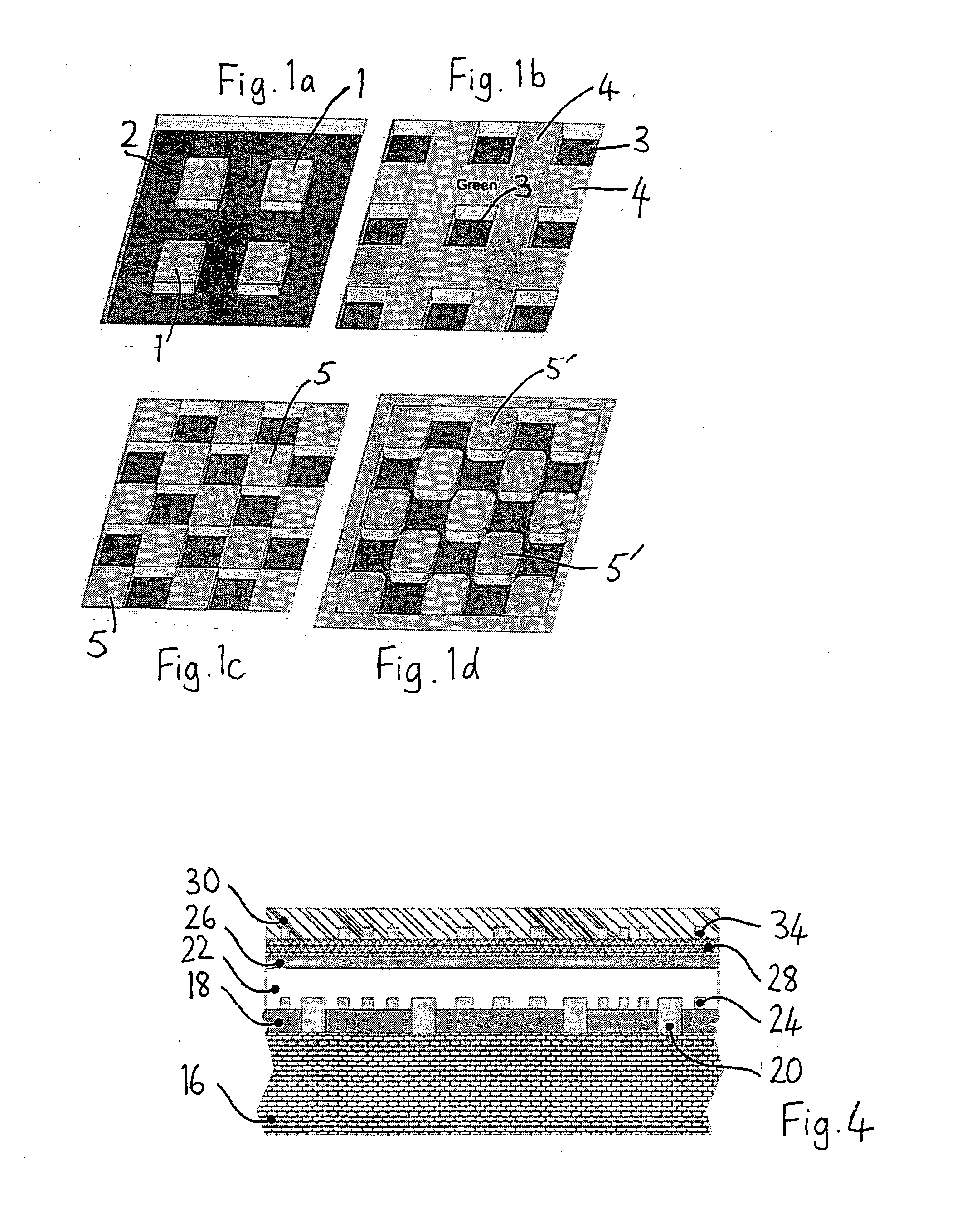
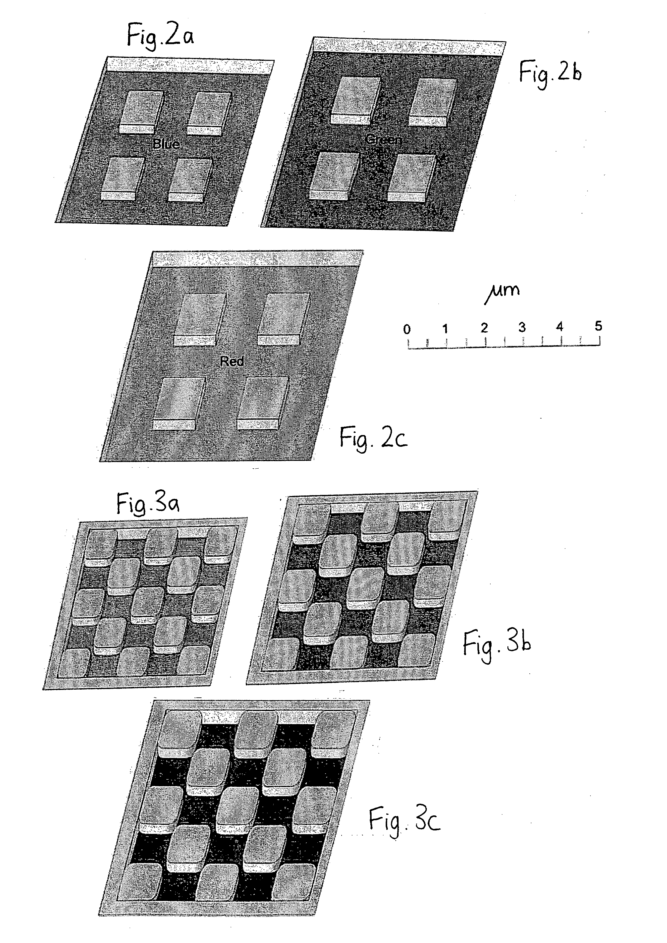
[0019]FIG. 1a shows a photonic lattice configured with pillars 1 of insulating material within an emissive area 2. FIG. 1b shows an alternative lattice with emitting sub-sub-pixels 3 confined with walls 4 of insulating material. FIG. 1c shows a lattice formed from a higher density matrix of pillars 5 and FIG. 1d shows a more realistic shape for the pillars 5′ fabricated by photolithography.

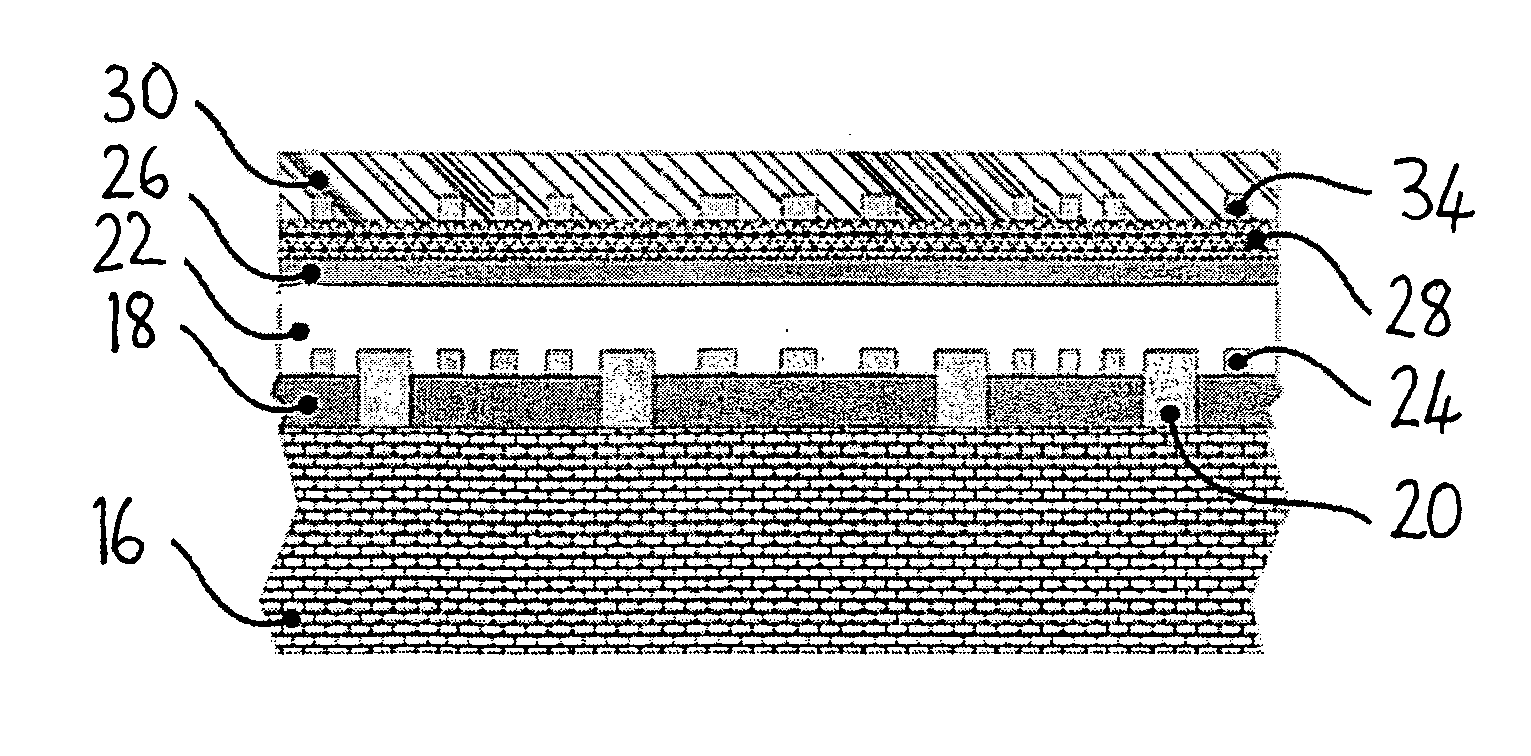
[0020]It is feasible to engineer such photonic lattice structures into a microdisplay device because semiconductor pattering technology, in particular CMOS technology, has the capability of patterning metal (typically aluminium) and insulator (silicon oxide or silicon nitride) to very high resolution (<0.5 μm).

[0021]Careful design of the spacing of a photonic lattice will provide enhanced out coupling of a certain wavelength of light. By engineering RGB sub-pixels to have difference and appropriate lattice spacing it is possible to enhance the outcoupling of a particular wavelength from each sub-p...


PUM


Abstract

An organic light emitting diode microdisplay device comprises a substrate including active circuitry (16) for addressing sub-pixels (10, 12, 14) of the device formed on the substrate, a metal anode layer (18), organic layers (22) at least including a light-emitting layer, a cathode layer (26) and encapsulation layers (28). The device includes at least one photonic lattice (24) having different, well-defined spacings for each sub-pixel that is arranged to emit light of a different colour. The device relies entirely on the photonic lattice (24) to determine the colour of light outcoupled from each sub-pixel.

Description

BACKGROUND TO THE INVENTION[0001]This invention relates to a microdisplay comprising organic light emitting diode (OLED) pixels.[0002]All LED devices suffer from the problem of light extraction. The root of the problem lies in traditional optics and the concept of total internal reflection. As all LED devices (OLED and inorganic LED) consist of stacks of thin films of high refractive index materials the chance of a photon escaping from the device is actually quite low and as such the external efficiency of the LED can be seriously limited. In traditional indicator LED's the problem is solved by capping the device with a hemispherical plastic shell to increase the number of angles capable of allowing light to pass. In OLED devices the solution is more complex as the LED device is typically required to be planar in its use as an information display.[0003]It is widely known that light outcoupling of OLED devices can be controlled in terms of magnitude by the insertion of 1D or 2D grati...

Claims


Application Information

Patent Timeline
IPC IPC(8): H01L33/52
CPCH01L51/5262H01L27/322H10K59/38H10K50/85H10K59/00H10K71/00
Inventor BUCKLEY, ALASTAIR ROBERTYATES, CHRISTOPHER
Owner MICROEMISSIVE DISPLAY
Why Eureka
Try Eureka