Organic-inorganic lighting device and a method for fabricating the same

a lighting device and organic-inorganic technology, applied in the field of lighting technology, can solve the problems of affecting the efficiency of the device, affecting the transmission of holes, and the number of electrons and holes in the device to be unbalanced, so as to achieve low electron mobility and reduce fabrication costs.

Inactive Publication Date: 2010-11-11
NAT TAIWAN UNIV
View PDF12 Cites 7 Cited by
  • Summary
  • Abstract
  • Description
  • Claims
  • Application Information

AI Technical Summary

Benefits of technology

[0008]An objective of the present invention is to provide an organic-inorganic lighting device and a method for fabricating the same, whereby a P-type organic conductive thin-film layer fabricated by a spin-coating method is combined with an N-type array of micro and nano zinc oxide wire of inorganic materials fabricated by a hydrothermal method. As a result, the difficult problems of low electron mobility in organic materials and epitaxial process of an inorganic diode in a vacuum and high-temperature environment with expensive equipment are solved, and the fabrication cost is greatly reduced.

Problems solved by technology

However, in the development of the OLED most organic materials are advantageous to the transmission of electrons but disadvantageous to the transmission of holes.
Therefore, this phenomenon can easily cause the number of electrons and holes in a device to be unbalanced and the efficiency of the device is affected.
On the contrary, inorganic materials of an inorganic diode are advantageous to the transmission of holes but disadvantageous to the transmission of electrons.
Additionally, in the general development of an inorganic lighting diode, the developer must consider the complicated and expensive epitaxial equipment and the process temperature of the epitaxial equipment which is more than 300° C. Therefore, the fabrication cost of an inorganic diode is very high.
For example, in the technology of the prior art, forming a zinc oxide thin-film on an organic layer made of MEHPPV [poly (2-methoxy-5-(2′-ethyl-hexyloxy)-1,4-phenylene vinylene) is fabricated by an electron beam evaporation method with high fabrication cost.

Method used


Image

  • Organic-inorganic lighting device and a method for fabricating the same
  • Organic-inorganic lighting device and a method for fabricating the same
  • Organic-inorganic lighting device and a method for fabricating the same

Examples


first embodiment

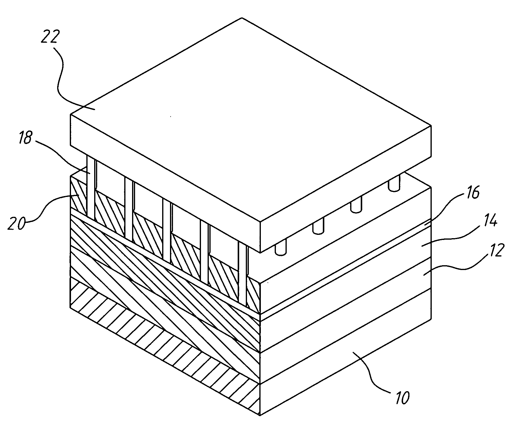
[0033]Refer to FIGS. 3(a)-3(k) for the method to fabricate the organic-inorganic lighting device of the As shown in FIG. 3(a), an insulation substrate 10 is provided firstly. Next, a first electrode layer 12, an organic conductive thin-film layer 14 and a seed layer 16 are sequentially formed on the insulation substrate 10. The organic conductive thin-film layer 14 is fabricated using one of the following methods: spin-coating method, dip-coating method, or ink printing method. The spin-coating method, dip-coating method and ink printing method require one of the following solutions: chloroform, dichloromethane, toluene, tetrahydrofuran, 1,2-dichlorobenzene, 1,4-dichlorobenzene, chlorobenzene, or n-hexane.

[0034]The seed layer 16 is fabricated using one of the following methods: spin-coating method, dip-coating method, evaporation method, sputtering method, atomic layer deposition method, electrochemical deposition method, pulsed laser deposition method, or metalorganic chemical vap...

second embodiment

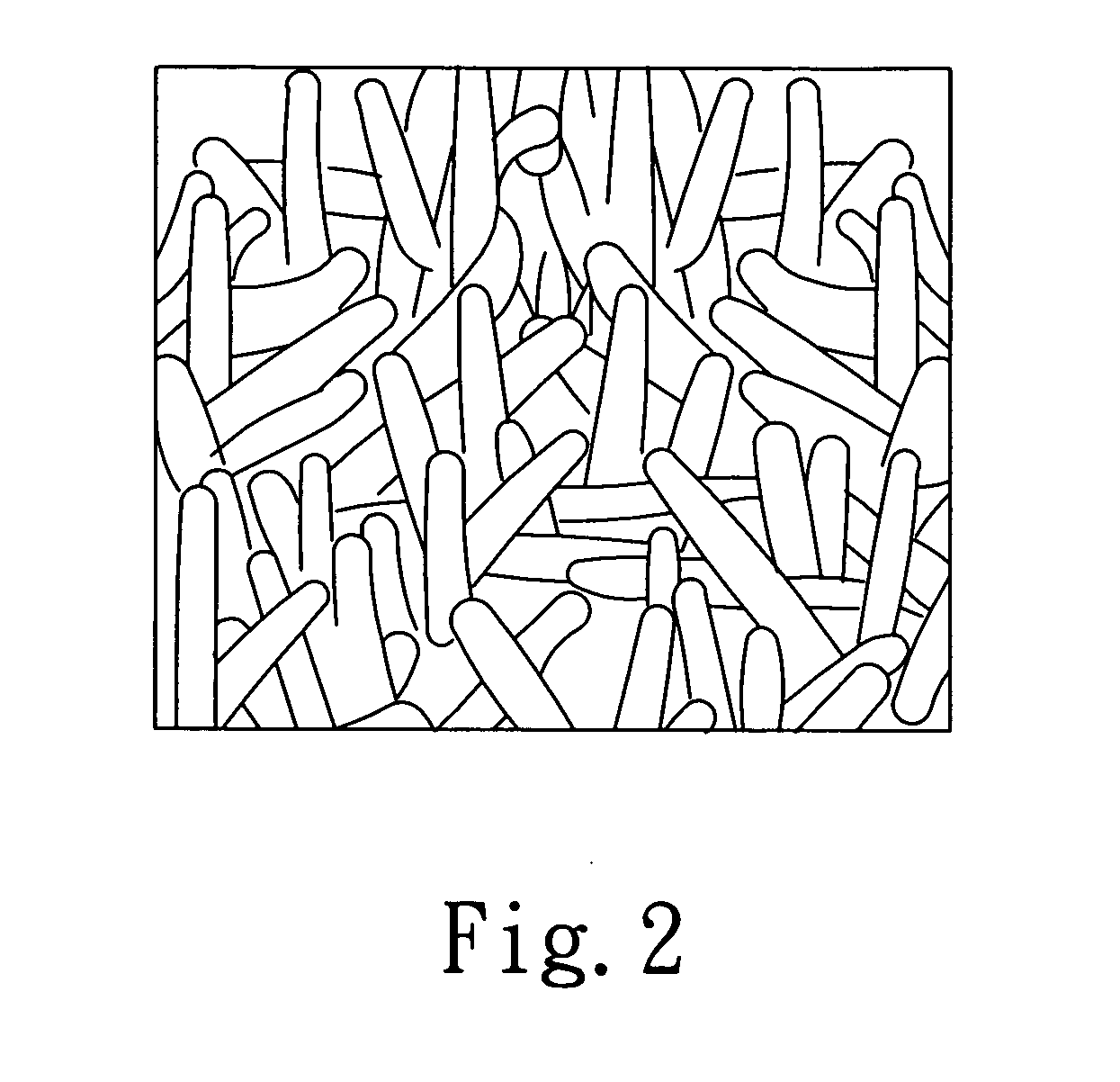
[0040]Refer to FIG. 4 for the present invention. The second embodiment is different from the first embodiment in that the first electrode layer 12 is divided into a plurality of first electrode blocks 24, and the first electrode blocks 24 are arranged equidistantly. The organic conductive thin-film layer 14 and the seed layer 16 are respectively divided into a plurality of organic blocks 26 and seed blocks 28; the array of micro and nano zinc oxide wire 18 is divided into a plurality of groups of micro array of zinc oxide 30, and the second electrode layer 22 is divided into a plurality of second electrode blocks 32. An organic block 26, a seed block 28, and a group of micro array of zinc oxide 30, are formed on each first electrode block 24 in order. The insulation layer 20 covers the seed layer 16 and the insulation substrate 10, and the top surface of the insulation layer 20 is lower than the tips of the array of micro and nano zinc oxide wire 18.

[0041]Refer to FIGS. 5(a)-5(e) fo...

third embodiment

[0042]Refer to FIG. 6 for the present invention. The third embodiment is different from the second embodiment in that a conductive substrate 34 replaces the insulation substrate 10 and the first electrode layer 12. The conductive substrate 34 has a plurality of conductive blocks 36 arranged equidistantly. An organic block 26, a seed block 28, and a group of micro array of zinc oxide 30, are formed on the each conductive block 36 in order.

[0043]Refer to FIGS. 7(a)-7(e) for the method of fabricating the organic-inorganic lighting device of the third embodiment. Firstly, as shown in FIG. 7(a), a conductive substrate 34 having a plurality of conductive blocks 36 arranged equidistantly is provided. Next, an organic block 26 and a seed layer 28 are sequentially formed on each conductive block 36. The steps shown in FIG. 7(b) to FIG. 7(e) are identical to the steps shown in FIG. 5(b) to FIG. 5(e), and have been described previously so will not be reiterated.

[0044]Below is a description of ...


PUM

PropertyMeasurementUnit
thicknessaaaaaaaaaa
thicknessaaaaaaaaaa
thicknessaaaaaaaaaa

Abstract

An organic-inorganic lighting device and a method for fabricating the same is disclosed. Firstly, a conductive substrate is provided, and an inorganic conducting film layer and a seed layer are formed in turn on the conductive substrate. Next, an array of micro and nano zinc oxide wire is formed on the seed layer by using properties of the seed layer. Finally, an electrode layer is formed on the array of micro and nano zinc oxide wire. The invention solves the problem of low mobility of electrons in inorganic materials.

Description

BACKGROUND OF THE INVENTION[0001]1. Field of the Invention[0002]The present invention relates to a lighting technology, particularly to an organic-inorganic lighting device and a method for fabricating the same.[0003]2. Description of the Related Art[0004]Since the LED was commercialized in 1960, LEDs have been used in many different devices, such as household appliances, indicators, or lighting sources for many kinds of instruments. This is because an LED has the following advantages: a high shake-enduring property, long life, lower power consumption, and a low heat-generating level. Because various colored and high intensity LEDs are now available, LEDs are now being utilized in outdoor displays, such as large-scale outdoor billboards, and traffic lights. Three primary colors of the visible light spectrum are red, yellow and blue. High intensity blue-light LEDs and green-light LEDs are essential for a full-color outdoor billboard.[0005]An OLED (Organic Light Emitting Diode) displa...

Claims


Application Information

Patent Timeline
Patent Type & Authority Applications(United States)
IPC IPC(8): H01J1/62B05D5/06B29D11/00C23C14/34C25D5/00C23C14/28H01J9/00H01L51/52H01L51/56
CPCH01L51/5048H05B33/26H01L2251/5369H10K50/14H10K2102/331
Inventor LIN, CHING-FUHLEE, CHUN-YU
Owner NAT TAIWAN UNIV
Why Eureka
Try Eureka