Semiconductor device and method of manufacturing the same

a semiconductor and chip technology, applied in the field of semiconductor devices, can solve problems such as defects on the semiconductor chip surface, and achieve the effect of improving the reliability of semiconductor devices

Active Publication Date: 2010-11-25
RENESAS ELECTRONICS CORP
View PDF7 Cites 22 Cited by
  • Summary
  • Abstract
  • Description
  • Claims
  • Application Information

AI Technical Summary

Benefits of technology

[0011]The present invention has been made in view of the above circumstances and provides a technique capable of suppressing a crack from occurring in a surface protective film and of improving the reliability of a semiconductor device even when a halogen-free member is used as a resin member to seal a semiconductor chip.
[0022]It is possible to improve reliability of a semiconductor device.

Problems solved by technology

At this time, if a halogen-free member is used as a resin member to seal the semiconductor chip, a defect of the semiconductor chip surfaces.

Method used


Image

  • Semiconductor device and method of manufacturing the same
  • Semiconductor device and method of manufacturing the same
  • Semiconductor device and method of manufacturing the same

Examples


first embodiment

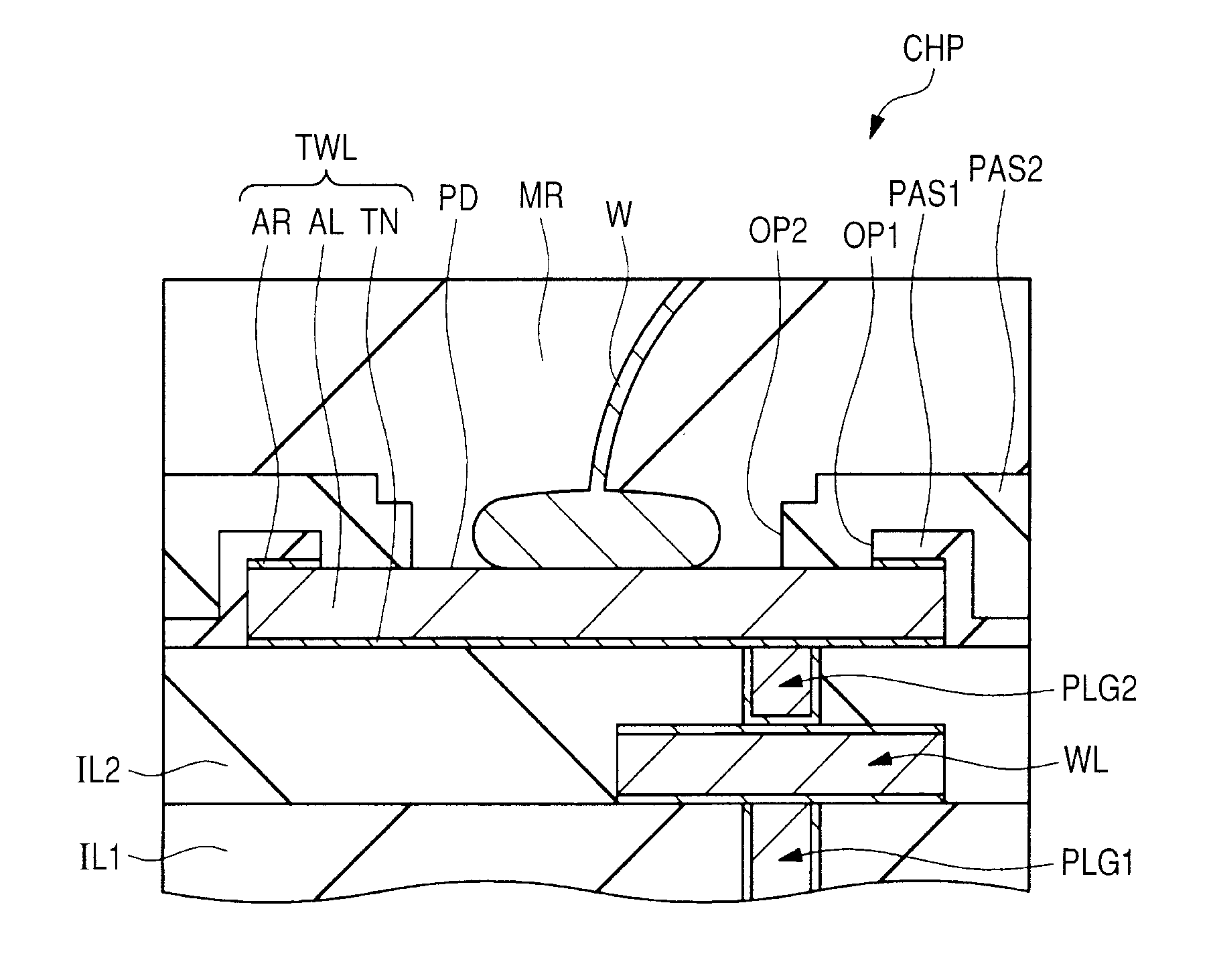
[0073]Before explaining a semiconductor device in a first embodiment, a new problem found by the inventors of the present invention is explained with reference to the drawings.

[0074]FIG. 1 is a section view showing a region that includes a pad formed in a conventional semiconductor chip. In FIG. 1, over a semiconductor substrate, not shown schematically, a semiconductor element, such as a MISFET (Metal Insulator Semiconductor Field Effect Transistor), is formed, and over the MISFET, a multilayer wire is formed. FIG. 1 shows a part in the vicinity of the uppermost layer of the multilayer wire. In FIG. 1, a plug PLG1 is formed in an interlayer insulating film IL1 and over the interlayer insulating film IL1 in which the plug PLG1 is formed, a wire WL is formed. The wire WL is electrically coupled with the plug PLG1. Then, over the interlayer insulating film IL1 over which the wire WL is formed, an interlayer insulating film IL2 is formed, and a plug PLG2 is formed in the interlayer ins...

second embodiment

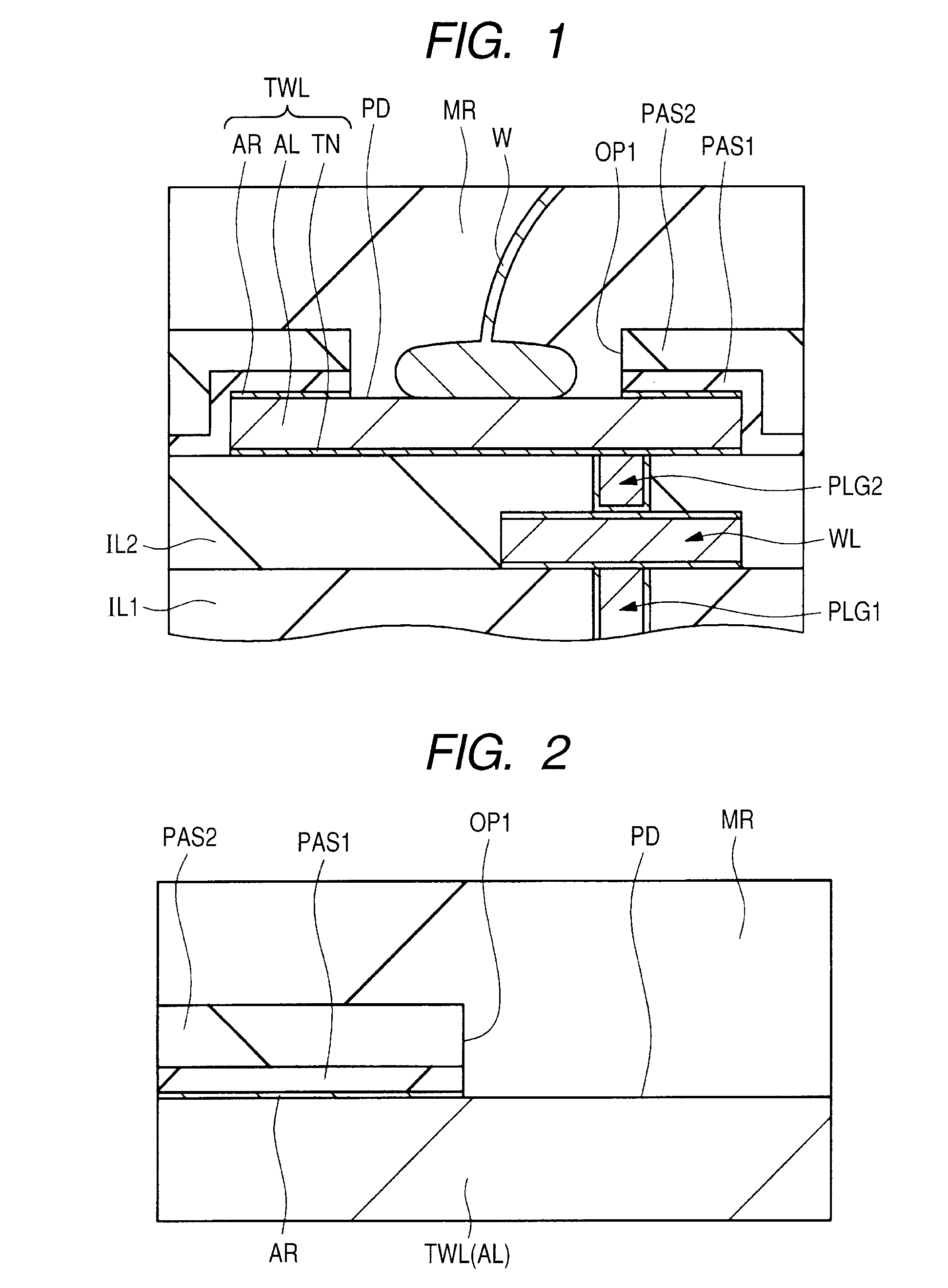
[0124]In the first embodiment described above, the opening OP1 is formed in the surface protective film PAS1 and after the antireflection film AR that is exposed at the bottom of the opening OP1 is removed, the opening OP2 is formed in the surface protective film PAS2. Then, by forming the opening OP2 in the surface protective film PAS2, the pad PD in which the aluminum film AL is exposed at the bottom of the opening OP2 is formed. At this time, the surface of the aluminum film AL that is exposed in the pad PD formation region is cleaned by removing the antireflection film AR that is exposed from the opening OP1 and further performing anti-corrosion processing.

[0125]However, in the present second embodiment, after that, over the aluminum film AL having the cleaned surface, the surface protective film PAS2 is formed and the opening OP2 is formed in the surface protective film PAS2. At this time, the aluminum film AL is exposed from the opening OP2, however, on the surface of the alum...

third embodiment

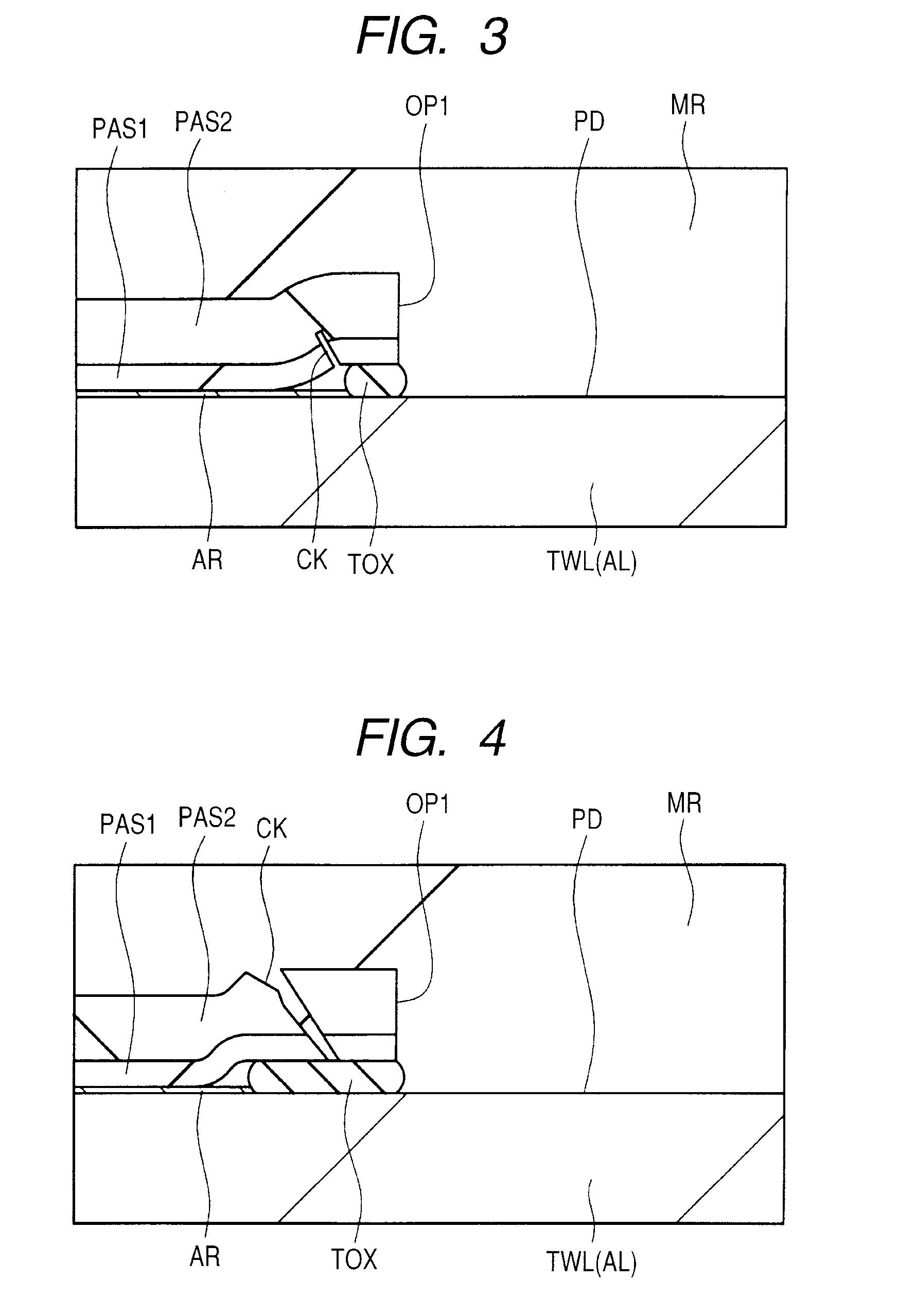
[0130]In the first embodiment described above, as shown in FIG. 8, the opening OP2 is formed so that the opening OP2 is included in the opening OP1 and the side surface of the opening OP1 at which the antireflection film AR is exposed is covered with the surface protective film PAS2. Due to such a configuration, in the first embodiment described above, in the voltage application test, the remarkable effect can be obtained that water that permeates the corner part of the opening OP2 can be prevented from coming into direct contact with the antireflection film AR that is exposed at the side surface of the opening OP1 and the occurrence of a large crack extending from the surface protective film PAS1 to the surface protective film PAS2 and the peeling of the antireflection film AR from the surface protective film PAS1 can be suppressed.

[0131]In a third embodiment, another effect is explained, which can be exhibited by further devising and improving the configuration in which the openin...


PUM

PropertyMeasurementUnit
temperatureaaaaaaaaaa
thicknessaaaaaaaaaa
thicknessaaaaaaaaaa

Abstract

To provide: a technique capable of suppressing a titanium nitride film that is exposed at the side surface of an opening from turning into a titanium oxide film even when water permeates the opening over a pad from outside a semiconductor device and thus improving the reliability of the semiconductor device; and a technique capable of suppressing a crack from occurring in a surface protective film of a pad and improving the reliability of a semiconductor device. An opening is formed so that the diameter of the opening is smaller than the diameter of another opening and the opening is included in the other opening. Due to this, it is possible to cover the side surface of an antireflection film that is exposed at the side surface of the other opening with a surface protective film in which the opening is formed. As a result of this, it is possible to form a pad without exposing the side surface of the antireflection film.

Description

CROSS-REFERENCE TO RELATED APPLICATION[0001]The disclosure of Japanese Patent Application No. 2009-121850 filed on May 20, 2009 including the specification, drawings and abstract is incorporated herein by reference in its entirety.BACKGROUND OF THE INVENTION[0002]The present invention relates to a semiconductor device and a method of forming the same, in particular, to technology which is effective when applied to a semiconductor device having a pad and the manufacturing technique of the same.[0003]Japanese Patent Laid-Open No. 2007-103593 (Patent Document 1) describes the technology capable of forming an opening of a protective film of a bonding pad for a laminated film including different kinds of metal film without diminution of the protective film and of avoiding the dissolution of the metal film in a step of immersing the metal film in an aqueous solution, such as a dicing step. Specifically, over the conductive film including an aluminum film and an antireflection film, such a...

Claims


Application Information

Patent Timeline
Patent Type & Authority Applications(United States)
IPC IPC(8): H01L23/48H01L21/60
CPCH01L22/32H01L23/293H01L23/3128H01L23/3135H01L23/562H01L23/564H01L24/03H01L24/05H01L24/45H01L24/48H01L24/97H01L2224/02166H01L2224/04042H01L2224/05073H01L2224/05166H01L2224/05187H01L2224/05567H01L2224/05571H01L2224/05624H01L2224/45124H01L2224/45144H01L2224/4807H01L2224/48091H01L2224/48227H01L2224/48465H01L2224/48624H01L2224/97H01L2924/01002H01L2924/01004H01L2924/01005H01L2924/01013H01L2924/01014H01L2924/01018H01L2924/01022H01L2924/01027H01L2924/01029H01L2924/01033H01L2924/01046H01L2924/0105H01L2924/01051H01L2924/01052H01L2924/01064H01L2924/01073H01L2924/01074H01L2924/01078H01L2924/01079H01L2924/014H01L2924/04941H01L2924/04953H01L2924/05042H01L2924/14H01L2924/15311H01L2924/01006H01L2224/48453H01L2224/32225H01L2224/73265H01L2224/48724H01L21/02697H01L2924/1306H01L2224/05553H01L2924/00014H01L2224/85H01L2924/00012H01L2924/00H01L24/73H01L2924/181H01L2224/05093H01L2224/0392H01L2924/10161H01L2224/023H01L2924/0001
Inventor HOMMA, TAKUROTAKATA, YOSHIFUMI
Owner RENESAS ELECTRONICS CORP
Why Eureka
Try Eureka