Optical Receiver Comprising Breakdown-Voltage Compensation

a technology of breakdown voltage and optical receiver, applied in the field of photodetectors, can solve problems such as inability to interrup

Active Publication Date: 2010-12-02
LG INNOTEK CO LTD
View PDF5 Cites 33 Cited by
  • Summary
  • Abstract
  • Description
  • Claims
  • Application Information

AI Technical Summary

Benefits of technology

[0021]The present invention provides an APD-based optical rec...

Problems solved by technology

For many applications, suc...

Method used


Image

  • Optical Receiver Comprising Breakdown-Voltage Compensation
  • Optical Receiver Comprising Breakdown-Voltage Compensation
  • Optical Receiver Comprising Breakdown-Voltage Compensation

Examples


Embodiment Construction

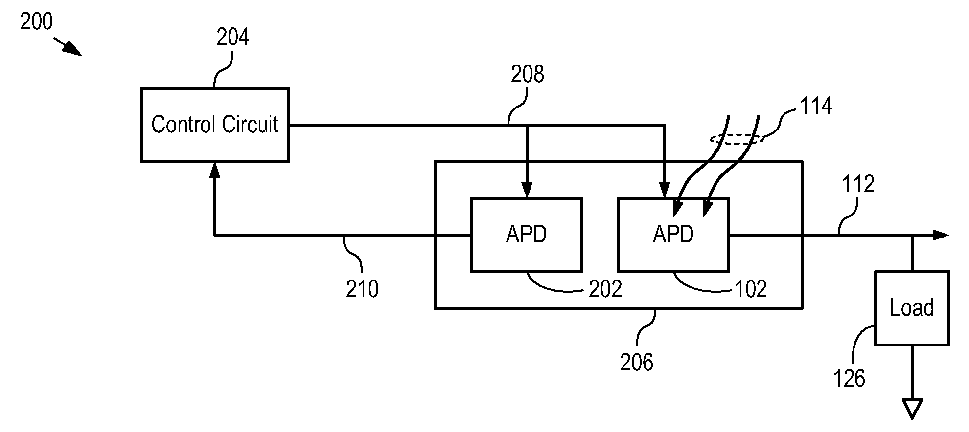
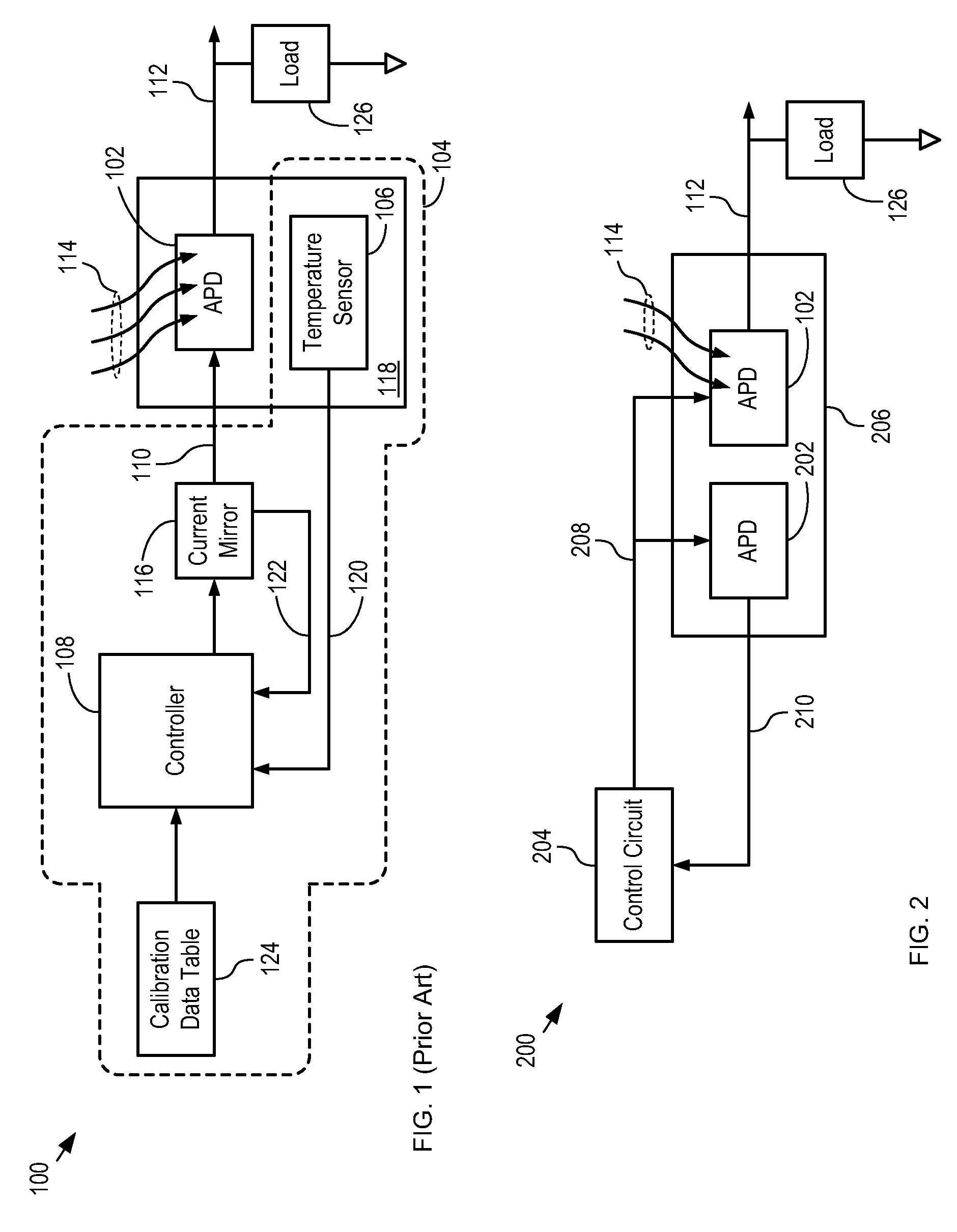
[0032]FIG. 1 depicts a schematic diagram of an optical receiver in accordance with the prior art. Optical receiver 100 comprises APD 102, temperature compensation circuit 104 and load 126.

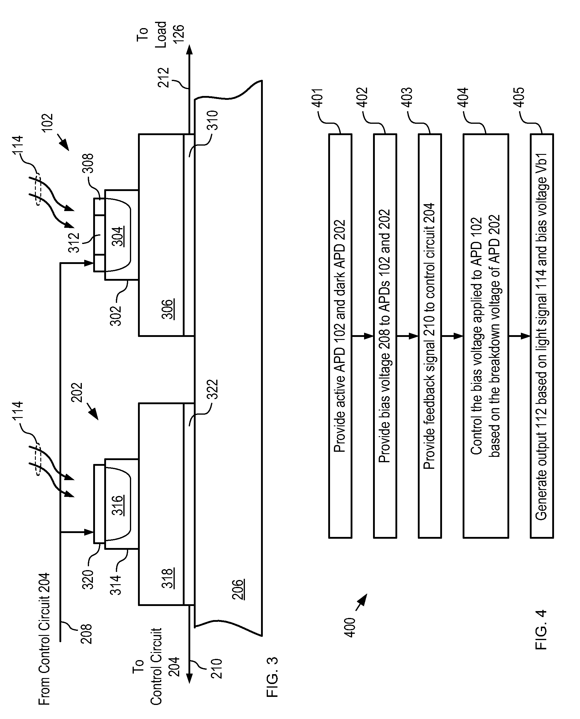
[0033]APD 102 is a conventional indium-phosphide-based avalanche photodiode designed for operation within the wavelength range of approximately 1000 nm to 1700 nm. APD 102 generates electrical output signal 112 in response to incident light signal 114. The gain of APD 102 is determined by the voltage with which it is biased. For the purposes of this Specification, including the appended claims, “bias voltage” is defined as the voltage potential induced between the cathode contact and anode contact of an APD. Electrical output signal 112, therefore, is based on the intensity of light signal 114 and voltage 110. Moreover, for the purposes of this Specification, including the appended claims, “offset voltage” is defined as the difference in voltage potential between the bias voltage and APD breakdown ...


PUM


Abstract

The present invention enables the detection of light using an APD that has high gain and/or a wide range of operating temperature. A first APD is biased with a voltage bias that is controlled based on the breakdown voltage of a second APD, which is thermally coupled with the first APD. Changes in the breakdown voltage of the second APD due to aging, temperature chances, and the like, are reflective of changes in the breakdown voltage of the first APD. As a result, the first APD can be operated with greater stability and reliability at high gain and over larger temperature excursions than APDs known in the prior art.

Description

CROSS REFERENCE TO RELATED APPLICATIONS[0001]This case claims priority of U.S. Provisional Patent Application U.S. 61 / 181,080, which was filed on May 26, 2009 (Attorney Docket: 293-021US), and which is incorporated herein by reference.FIELD OF THE INVENTION[0002]The present invention relates to photodetectors in general, and, more particularly, to avalanche photodiodes.BACKGROUND OF THE INVENTION[0003]A semiconductor photodiode is a device that provides an electric current in response to the absorption of light. Photodiodes are used in myriad applications, such as optical communications applications, sensing applications, industrial control applications, and security applications.[0004]A photodiode provides an electric current is based upon a process known as “photo-absorption,” in which the photodiode generates a free-carrier pair (an electron and a hole) when it absorbs a particle of light (i.e., photon). To generate a free-carrier pair, an incident photon having sufficient energy...

Claims


Application Information

Patent Timeline
IPC IPC(8): H01L27/144H01L31/107
CPCG01J1/18H01L31/02027G01J1/44G01J1/4228
Inventor PATEL, KETAN MUKUNDITZLER, MARK ALLEN
Owner LG INNOTEK CO LTD
Why Eureka
Try Eureka