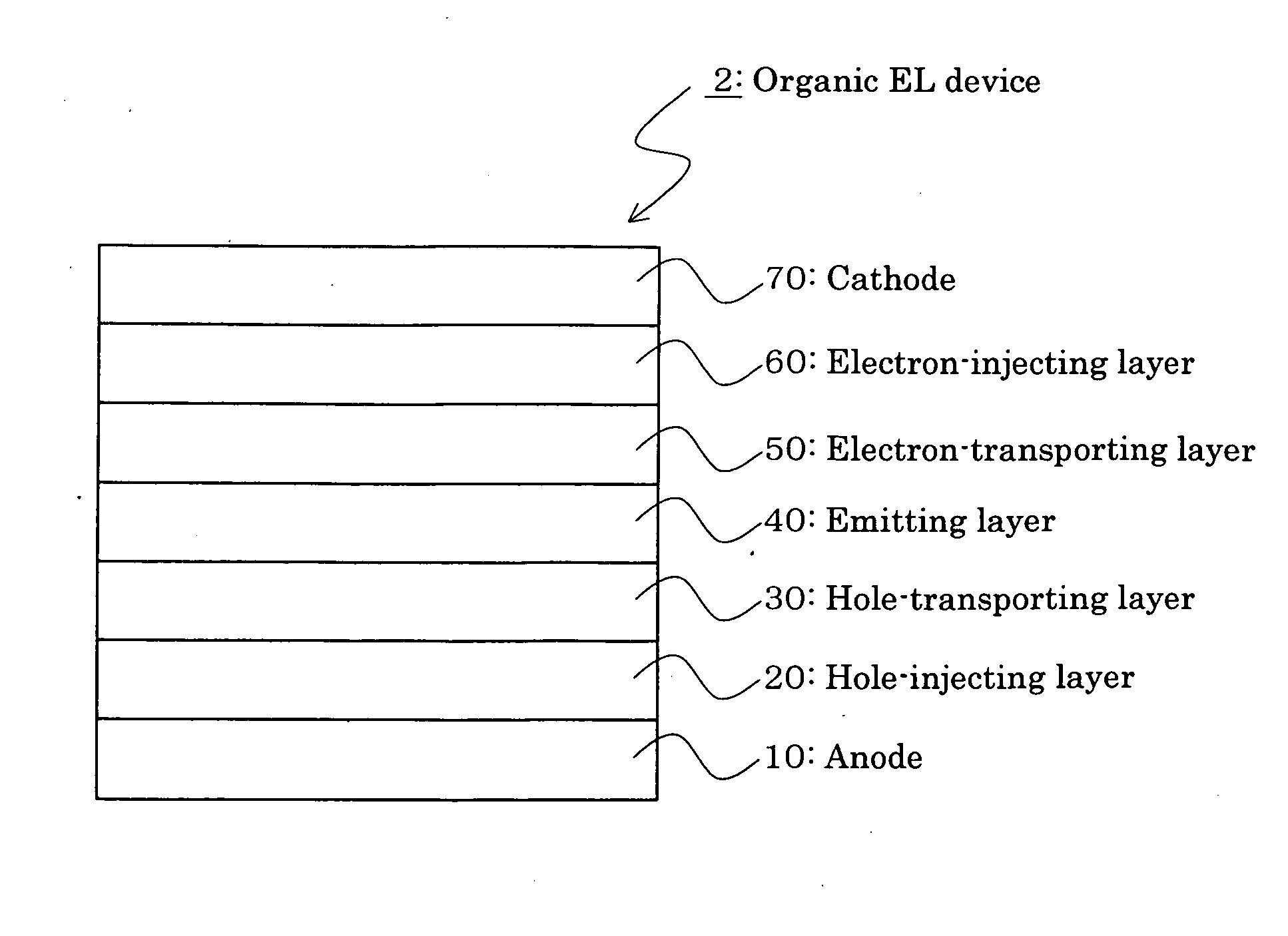
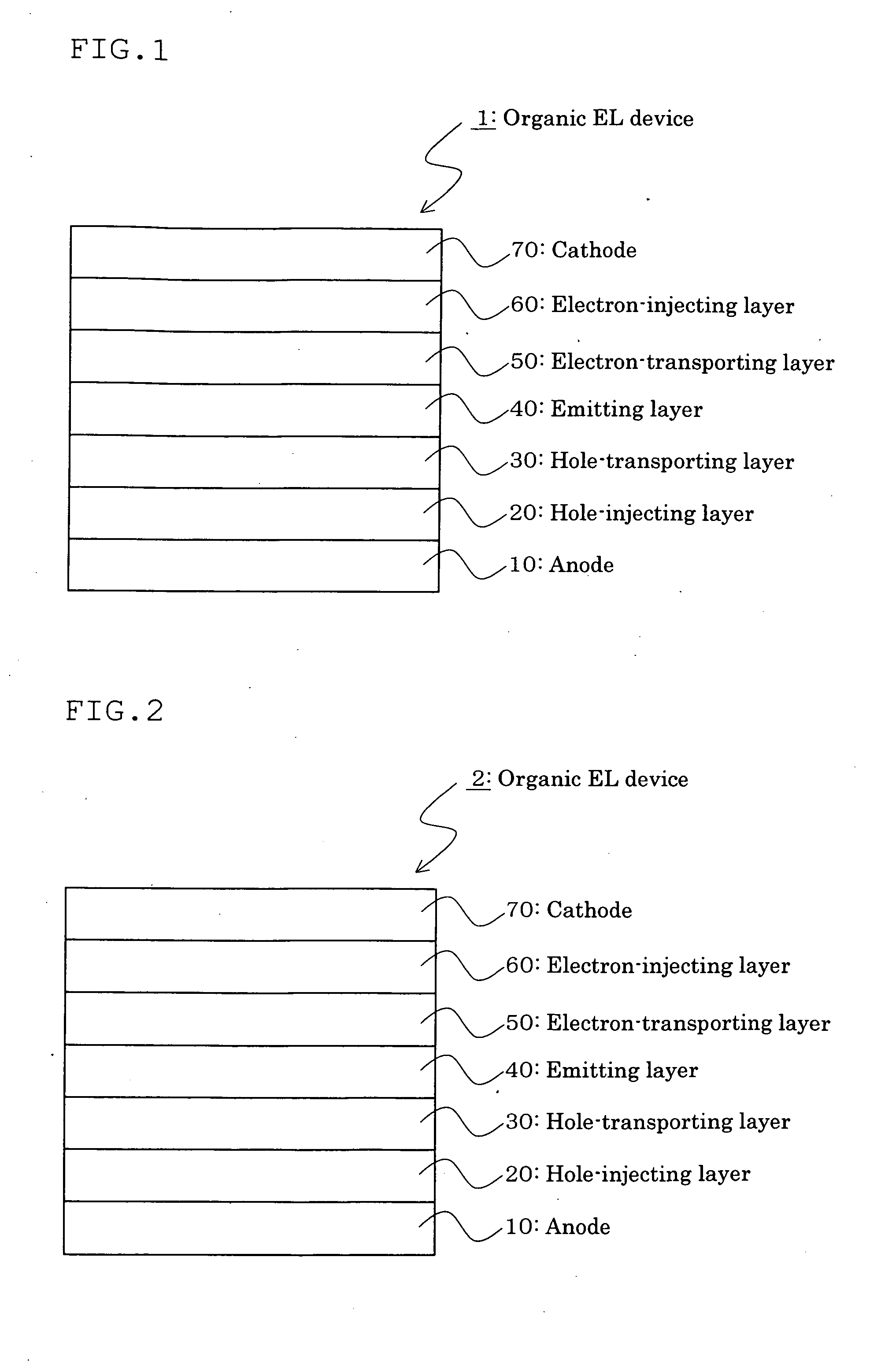
Organic electroluminescence device
an electroluminescence device and organic technology, applied in thermoelectric devices, triarylamine dyes, nanoinformatics, etc., can solve the problems of insufficient luminous efficiency and life time of the meterial system disclosed in patent document 8 and the significant increase in the driving voltage, etc., to achieve high efficiency, long life time, and high efficiency
- Summary
- Abstract
- Description
- Claims
- Application Information
AI Technical Summary
Benefits of technology
Problems solved by technology
Method used
Image

Examples
example 1
[0316]A glass substrate of 25 mm by 75 mm by 1.1 mm thick with an ITO transparent electrode (GEOMATEC Co., LTD.) was subjected to ultrasonic cleaning with isopropyl alcohol for 5 minutes, and cleaned with ultraviolet rays and ozone for 30 minutes. The resultant substrate with transparent electrode lines was mounted on a substrate holder in a vacuum vapor deposition device. First, as a hole-injecting layer, compound HI1 film was formed into a film at a film-forming rate of 1 Å / s in a thickness of 10 nm so as to cover the surface of the transparence electrode on which the transparence electrode lines were formed. On the film of the compound H1, as a hole-transporting layer, a 35 nm-thick film of compound HT1 was formed at 1 Å / s.
[0317]Furthermore, on the film of the compound H1, compound L1 and compound L2 were formed into a 20 nm-thick film such that the thickness ratio became 18:2. This film functioned as a blue emitting layer. The film-forming rate was 1 Å / s and 0.11 Å / s, respective...
example 2
[0319]An organic EL device was fabricated in the same manner as in Example 1, except that compound HT2 was stacked in a film thickness of 35 nm as a hole-transporting layer.
example 3
[0320]An organic EL device was fabricated in the same manner as in Example 1, except that compound ET2 was stacked in a film thickness of 30 nm as an electron-transporting layer.
PUM
 Abstract
Description
Claims
Application Information