Chip-based advanced modulation format transmitter

a technology of advanced modulation and transmitter, applied in multiplex communication, manufacturing tools, instruments, etc., can solve the problems of large-scale pics that may require low waveguide losses, high-performance optical sources and other optical subcomponents, etc., to reduce fabrication complexity, reduce footprint and/or die size, and reduce the effect of die siz

Active Publication Date: 2010-12-02
FREEDOM PHOTONICS LLC
View PDF71 Cites 85 Cited by
  • Summary
  • Abstract
  • Description
  • Claims
  • Application Information

AI Technical Summary

Benefits of technology

[0008]Various embodiments described herein include a compact optical transmitter having a reduced die size. For example, the die size of the various embodiments of the optical transmitter device described herein can be between approximately 0.5 square mm and approximately 3 square mm. In various embodiments, the die size of the optical transmitter device can be between approximately 1.5 square mm and approximately 2.5 square mm. In various embodiments, the die comprises a monolithically integrated optical transmitter device that is included in packaging to form the device. In various embodiments, the die can comprise a monolithically integrated optical transmitter device that will be coupled to optical fibers or RF / electrical connectors. The decrease in the footprint and / or the die size of the optical transmitter device can advantageously reduce fabrication complexity required to integrate a single surface-ridge waveguide structure and improve yield. Various embodiments of the optical transmitter described herein can comprise a tunable laser resonator and an optical vector modulator. In various embodiments, an optical vector modulator can include a modulator arrangement capable of modulating both optical intensity and optical phase to generate optical vector modulation. Examples of optical vector modulation formats include QPSK modulation and multilevel QAM modulation. An arrangement for passive modulator bias control can be implemented in various embodiments of the optical transmitter to adjust for the wavelength dependence of the modulator.
[0009]In various embodiments described herein, an optical transmitter comprising a widely tunable laser and one or more optical vector modulators may be monolithically integrated on a single die having a common substrate. In various embodiments, monolithic common substrate integration can include processes and techniques that place all the subcomponents of the device on a common substrate through semiconductor device processing techniques (e.g. deposition, epitaxial growth, wafer bonding, wafer fusion, etc). In some embodiments, the optical transmitter comprising a widely tunable laser and one or more optical vector modulators may be integrated on a single die having a common substrate, through other techniques such as flip-chip bonding, etc. Monolithic common substrate integration can provide a reduction in device insertion losses. Such tunable optical transmitter devices can allow for a reduction in the number of components and devices required in an optical system. Other advantages of an integrated tunable optical transmitter can be compact die size, reduced footprint, faster tuning mechanisms, and the lack of moving parts—which can be desirable for applications subject to shock, vibration or temperature variation. Integrating an optical transmitter on a single die can offer several other advantages as well, such as precise phase control, improved performance and stability of the transmitter, and compact implementation. Some additional benefits of integrating a tunable laser with an optical modulator on a single die can be: the ability to adjust or optimize the device performance; ability to control and optimize the bias of the modulators for every single wavelength—(the wavelength information is known for an integrated transmitter, but not known when a discrete modulator is used); and ability to utilize feedback from on-chip integrated tap signals in order to better control the operating point of the chip.
[0010]Various embodiments, described herein include a complex optical transmitter fabricated on a small die size. Such devices can be fabricated using relatively simple fabrication techniques and / or integration platforms. In various embodiments described herein, optical interconnect losses can be reduced by reducing interconnect length rather than by including complex low-loss optical waveguide structures.

Problems solved by technology

Due to their size, large-scale PICs may require low waveguide losses, high performance optical sources and other optical subcomponents.

Method used


Image

  • Chip-based advanced modulation format transmitter
  • Chip-based advanced modulation format transmitter
  • Chip-based advanced modulation format transmitter

Examples


Embodiment Construction

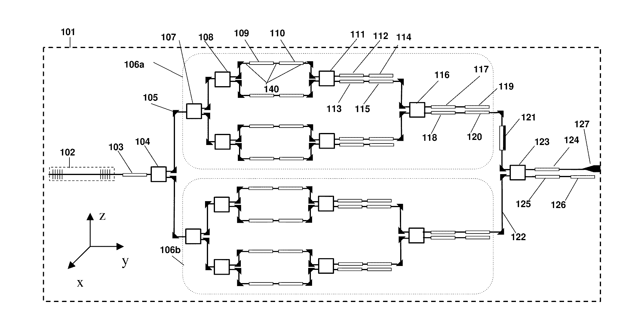
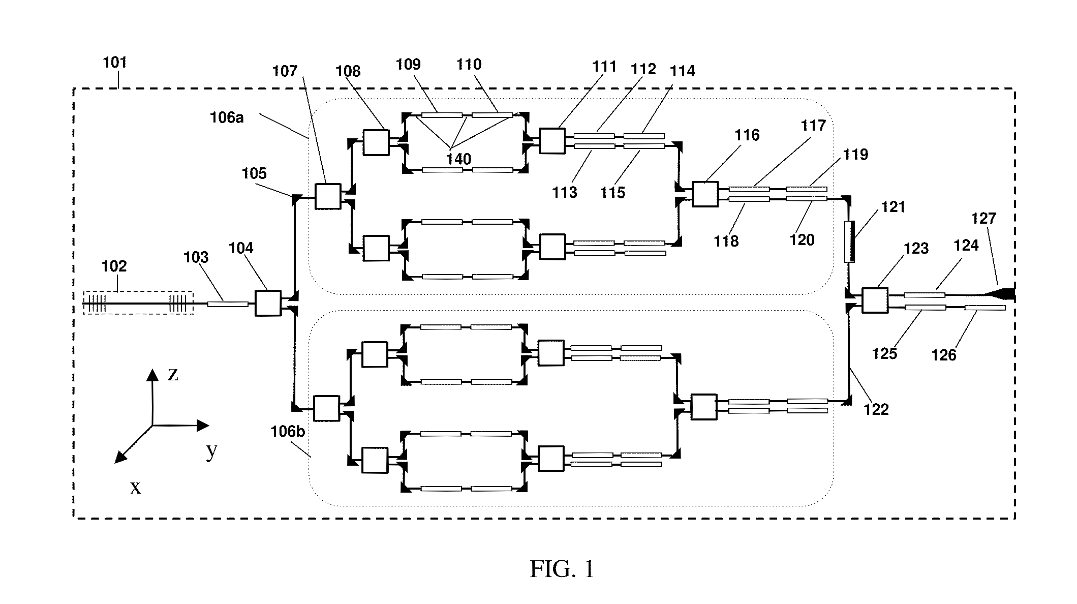
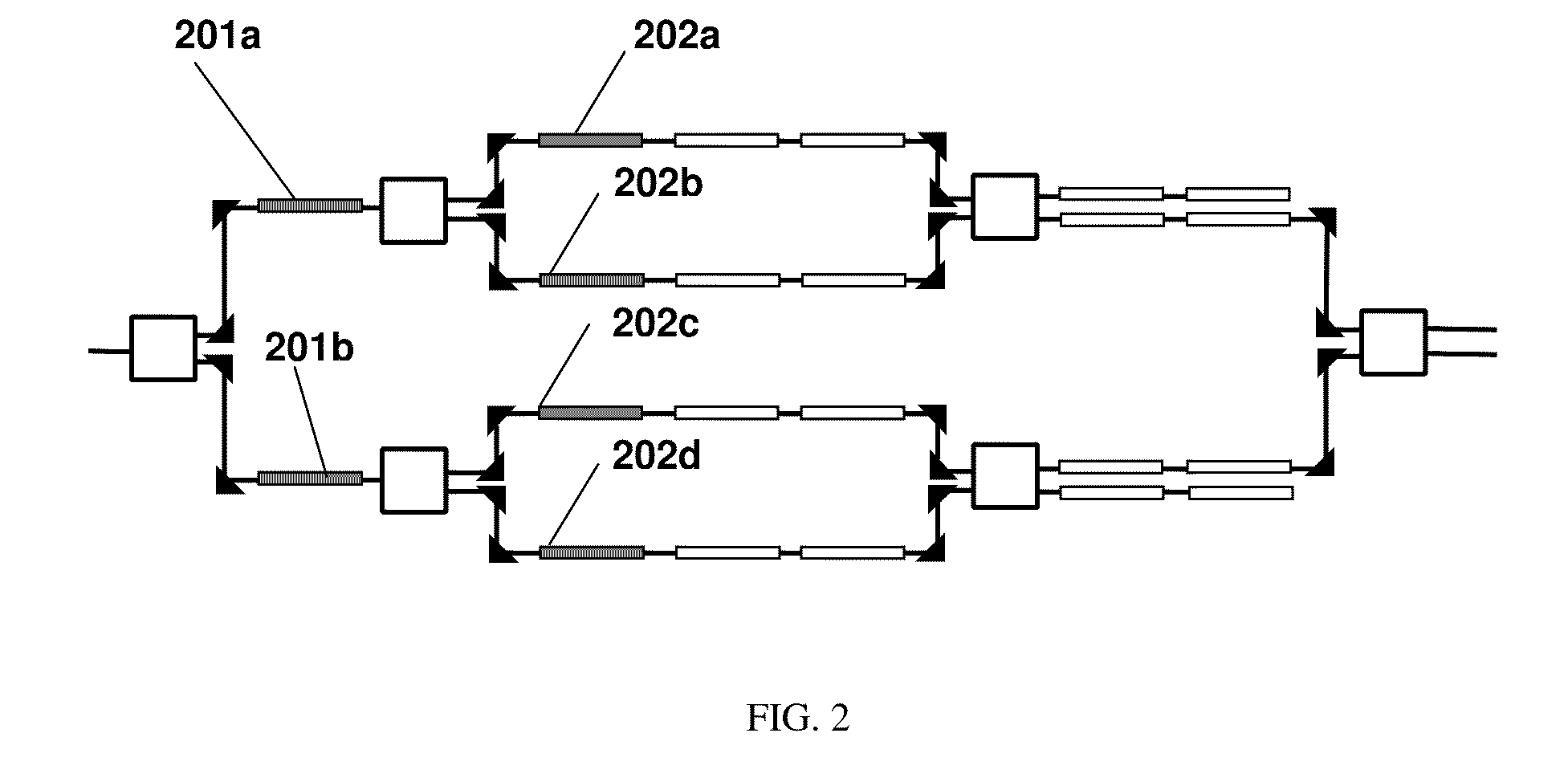
[0026]Although certain preferred embodiments and examples are disclosed below, inventive subject matter extends beyond the specifically disclosed embodiments to other alternative embodiments and / or uses and to modifications and equivalents thereof. Thus, the scope of the claims appended hereto is not limited by any of the particular embodiments described below. For example, in any method or process disclosed herein, the acts or operations of the method or process may be performed in any suitable sequence and are not necessarily limited to any particular disclosed sequence. Various operations may be described as multiple discrete operations in turn, in a manner that may be helpful in understanding certain embodiments; however, the order of description should not be construed to imply that these operations are order dependent. Additionally, the structures, systems, and / or devices described herein may be embodied using a variety of techniques including techniques that may not be descri...


PUM

PropertyMeasurementUnit
angleaaaaaaaaaa
angleaaaaaaaaaa
angleaaaaaaaaaa

Abstract

In various embodiments, a monolithic integrated transmitter, comprising an on-chip laser source and a modulator structure capable of generating advanced modulation format signals based on amplitude and phase modulation are described.

Description

CROSS-REFERENCE TO RELATED APPLICATIONS[0001]This application claims the benefit under 35 U.S.C. §119(e) of U.S. Provisional Application 61 / 182,017 filed on May 28, 2009 titled “Chip-Based Advanced Modulation Format Transmitter,” which is hereby expressly incorporated herein by reference in its entirety.[0002]This application also claims the benefit under 35 U.S.C. §119(e) of U.S. Provisional Application 61 / 182,022 filed on May 28, 2009 titled “Monolithic Widely-Tunable Coherent Receiver,” which is hereby expressly incorporated herein by reference in its entirety.BACKGROUND[0003]1. Field of the Invention[0004]Various embodiments of the invention relate to the area of optical communications photonic integrated circuits (PICs). In particular, various embodiments relate to integrated optical transmitters capable of generating multilevel optical modulation formats in optical communications applications.[0005]2. Description of the Related Art[0006]As demand for higher capacity in optical...

Claims


Application Information

Patent Timeline
Patent Type & Authority Applications(United States)
IPC IPC(8): H04B10/04B23P11/00
CPCH04B10/505H04B10/516H04B10/5161H04B10/615H04B10/6151H04B10/801G02F2001/212Y10T29/49826G02B2006/12104G02B6/2766G02B6/125G02F1/2257G02F1/2255H04B10/503G02F1/212
Inventor BARTON, JONATHONJOHANSSON, LEIFMASHANOVITCH, MILAN
Owner FREEDOM PHOTONICS LLC
Why Eureka
Try Eureka