(110) dislocation-free monocrystalline silicon and its preparation and the graphite heat system used

a technology of monocrystalline silicon and graphite, which is applied in the direction of crystal growth process, polycrystalline material growth, crystal growth process, etc., can solve the problems of single crystal fundamental limitations, and achieve the effect of speeding up the speed of shoulder expansion

Inactive Publication Date: 2010-12-09
TIANJIN HUANOU SEMICON MATERIAL TECH CO LTD
View PDF2 Cites 5 Cited by
  • Summary
  • Abstract
  • Description
  • Claims
  • Application Information

AI Technical Summary

Benefits of technology

[0020](7) rotate shoulder: speeding up the speed of shoulder-expanding;
[0021](8)

Problems solved by technology

The production of (110) single crystal with traditional pulling technique, has dislocation limitation as well, thus, in order to produce (110) dislocation-free monocrystalline silicon, the dislocation should be eliminated but it is a techn

Method used


Image

  • (110) dislocation-free monocrystalline silicon and its preparation and the graphite heat system used
  • (110) dislocation-free monocrystalline silicon and its preparation and the graphite heat system used
  • (110) dislocation-free monocrystalline silicon and its preparation and the graphite heat system used

Examples


Embodiment Construction

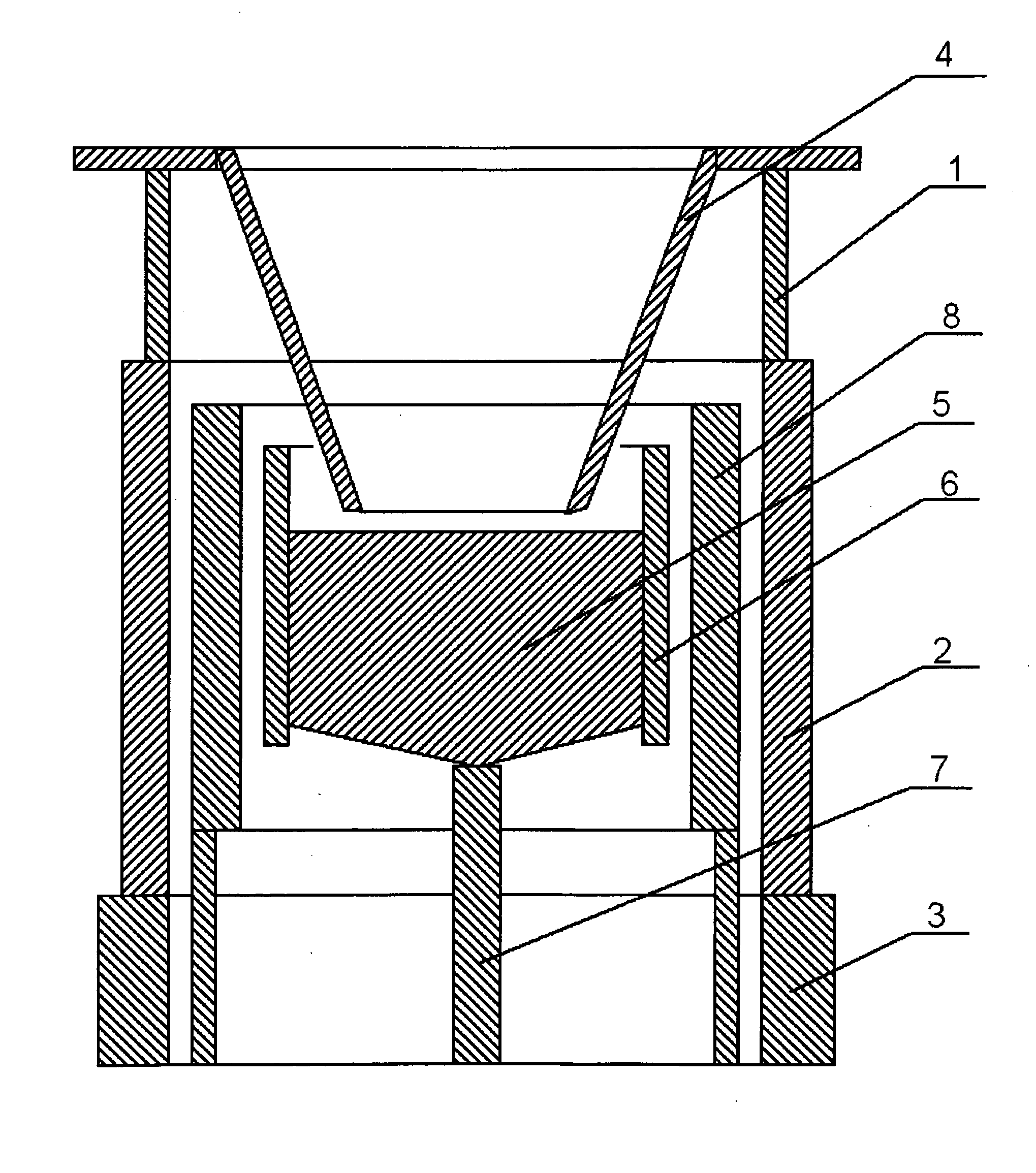
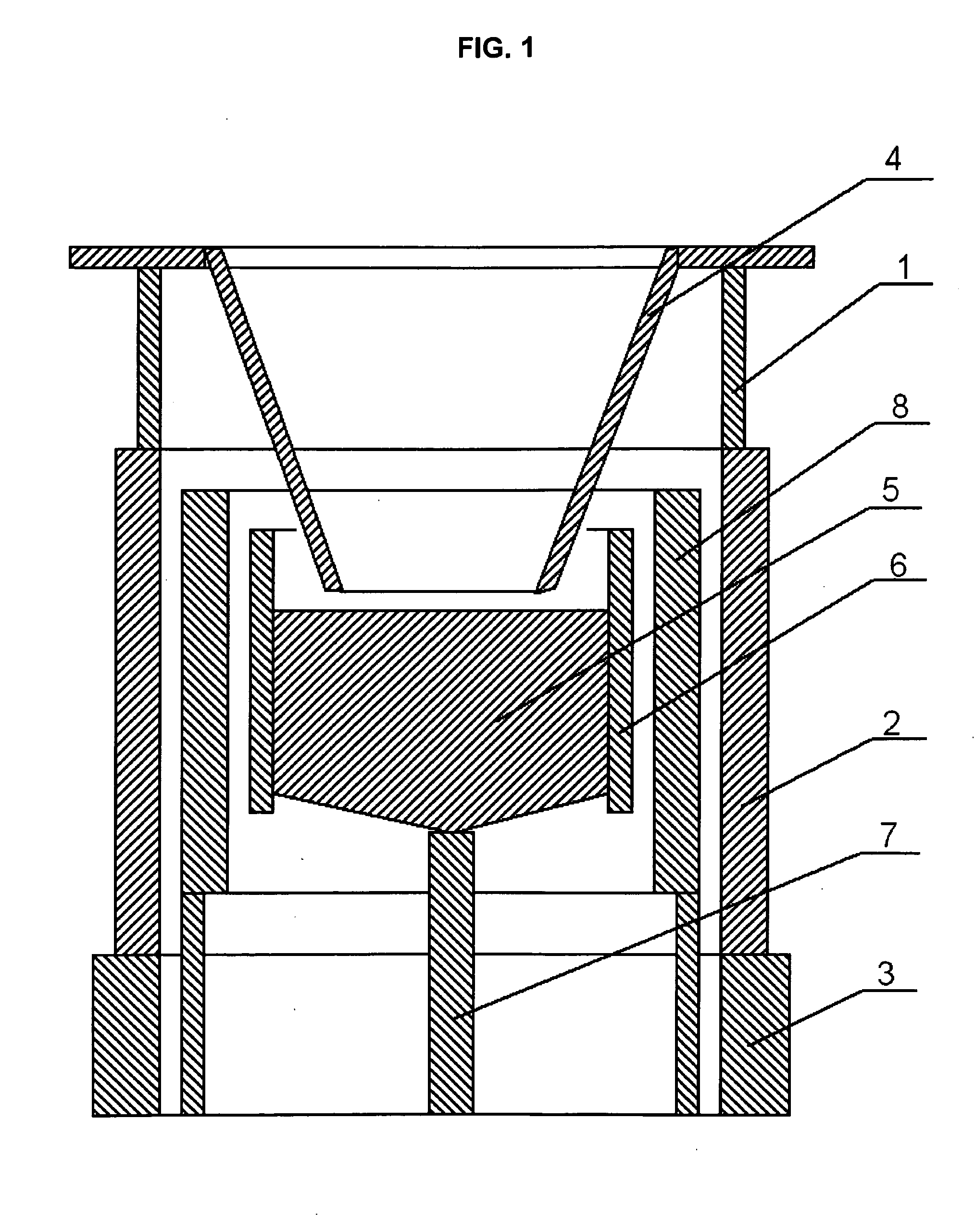
[0039]The (110) dislocation-free monocrystalline silicon and its preparation and the graphite heating system to be used in the invention (for example, 6 inch (110) dislocation-free monocrystalline silicon) are further illustrated by combining some preferred embodiments.

[0040]The process for producing (110) dislocation-free monocrystalline silicon of the invention, is to complete the preparation work at first, including: clean the room, wear the work clothes and gloves, cap and respirator. Turn on the main power of the single crystal furnace, start up the main power of the control screen, each indicator is indicative and able to work, particularly including the following steps:

[0041](1) clean the furnace and tidy the heat field:

[0042]1) make sure the isolating valve is open, open the valve of the argon flowmeter, charge argon into the hearth, observe the pressure gauge on the left of the sub-furnace room. If the pressure inside the furnace is the same as ambient air pressure, i.e. th...


PUM


Abstract

The invention discloses (110) dislocation-free monocrystalline silicon and its preparation and the graphite heating system used. The process for preparation is as follows: clearing furnace and tidy the heat field; loading furnace; vacuumizing and argon charging; heating raw material; crystal seeding; expanding shoulder; rotating shoulder: speeding up the speed of shoulder-expanding; equal diameter: after shoulder-rotating, stabilize the crystal growth speed; finishing: turning off the power of crucible, decreasing the drawing rate manually; turning off the furnace. The graphite heating system includes: upper insulation column, lower insulation column and hearth tray arranged from the top down to form the external shell, and the peripheral surface is a stepped structure, and the thickness of the insulation layer of the upper insulation column is 20-30 mm, the thickness of the insulation layer of the lower insulation column is 60-70 mm, and the thickness of the insulation layer of the hearth tray is 70-80 mm. (110) dislocation-free monocrystalline silicon is cylinder structure, on its expanded shoulders 2 symmetrical main crest lines and 4 symmetrical sub-crest lines are formed, and 2 symmetrical main crest lines are formed on crystal cylinder surface. The present invention realizes manufacturing (110) dislocation-free monocrystalline silicon so as to meet the demand of the domestic and international markets.

Description

FILED OF THE INVENTION[0001]The present invention relates to a pulling crystal technique, especially a (110) dislocation-free monocrystalline silicon suitable for special semiconductor and solar photoelectric devices and its preparation and the graphite heating system to be used.BACKGROUND OF THE INVENTION[0002]It is well known, in silicon crystal lattice, since the angle between (110) crystal face and (111) crystal face is 90° and 35° 16′, dislocation on (111) crystal face with angle of 90° is the same as (110) lattice orientation. The production of (110) single crystal with traditional pulling technique, has dislocation limitation as well, thus, in order to produce (110) dislocation-free monocrystalline silicon, the dislocation should be eliminated but it is a technical problem in pulling technique all along.[0003]Uses of improving drawing rate greatly, controlling diameter and length of crystal seed and, controlling shoulder-expanding speed, increasing the finish length of single...

Claims


Application Information

Patent Timeline
IPC IPC(8): C30B15/22C30B15/14
CPCC30B15/14Y10T117/1068C30B35/00C30B29/06
Inventor SHEN, HAOPINGWANG, YUTIANHU, YUANQINGSHANG, WEIZELI, XIANGLI, HAIJINGSI, WEIGAO, RUNFEI
Owner TIANJIN HUANOU SEMICON MATERIAL TECH CO LTD
Why Eureka
Try Eureka