ZnO-BASED SUBSTRATE, METHOD FOR PROCESSING ZnO-BASED SUBSTRATE, AND ZnO-BASED SEMICONDUCTOR DEVICE

a technology of zno-based substrates and substrates, which is applied in the direction of crystal growth process, polycrystalline material growth, after-treatment details, etc., can solve the problems of p-type zno, use of specials, and no significant development of such a zno-based semiconductor as a semiconductor device material, etc., to improve the quality of the substrate surface and enhance the cleanness of the surface of the zno-based substrates.

Inactive Publication Date: 2010-12-09
ROHM CO LTD
View PDF2 Cites 7 Cited by
  • Summary
  • Abstract
  • Description
  • Claims
  • Application Information

AI Technical Summary

Benefits of technology

[0023]The ZnO-based substrate of the present invention is configured such that any one of a carboxyl group and a carbonate group is substantially absent in a principal surface on a side where crystal growth takes place. This makes it possible to enhance the cleanness of the surface of the ZnO-based substrate and therefore to fabricate a high-quality ZnO-based thin film on the substrate. Meanwhile, in order for a carboxyl group or a carbonate group to be substantially absent, any one of oxygen radicals, oxygen plasma and ozone is brought into contact with the surface of the ZnO-based substrate before the crystal growth is started. This cleans the surface of the ZnO-based substrate and therefore improves the quality of the substrate surface.

Problems solved by technology

However, no significant development has been made on such a ZnO-based semiconductor as a semiconductor device material.
The largest obstacle is that p-type ZnO cannot be obtained because of difficulty in acceptor doping.
Nonetheless, use of a special and insulative ScAlMgO4 substrate as well as pulsed laser deposition which is a method unsuitable for a large area is disadvantageous in term of industrial application.
However, a substrate surface is the most problematic part in the case of fabricating a device demonstrating a new function by stacking films different not only in dopant but in composition, as in cases of many compound semiconductors.
Thus, even when the bulk has a high quality, the substrate is totally meaningless if the surface does not have a sufficiently high quality.
Poor flatness in a substrate surface leads to poor flatness in a film stacked thereon, which in turn works as resistance to carriers moving through the thin film.
In addition, the higher the layer in a stacked structure becomes, the larger the surface roughness becomes.
Such surface roughness is likely to cause a problem of an uneven etching depth.
The surface roughness is also likely to cause a problem of anisotropic crystal surface growth.
Thus, a semiconductor device is likely to have a difficulty in demonstrating a desired function.

Method used


Image

  • ZnO-BASED SUBSTRATE, METHOD FOR PROCESSING ZnO-BASED SUBSTRATE, AND ZnO-BASED SEMICONDUCTOR DEVICE
  • ZnO-BASED SUBSTRATE, METHOD FOR PROCESSING ZnO-BASED SUBSTRATE, AND ZnO-BASED SEMICONDUCTOR DEVICE
  • ZnO-BASED SUBSTRATE, METHOD FOR PROCESSING ZnO-BASED SUBSTRATE, AND ZnO-BASED SEMICONDUCTOR DEVICE

Examples


Embodiment Construction

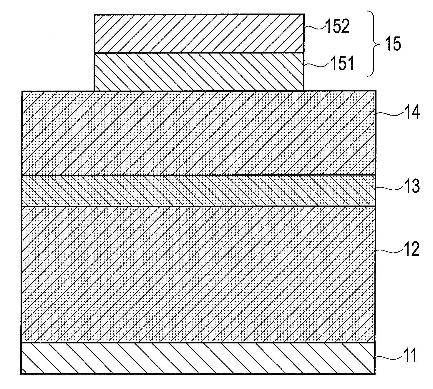
[0038]First of all, a ZnO-based substrate is a substrate mainly containing ZnO and is formed of ZnO or a compound containing ZnO. Besides one containing ZnO, a specific example of the substrate includes one containing any one of oxides of: a group IIA element and Zn; a group IIB element and Zn; a group IIA element, a group IIB element and Zn. Mix crystals such as MgXZn1-XO in which Mg is mixed in order to widen the bandgap are also included.

[0039]In this embodiment, a MgXZn1-XO substrate (0≦X≦1) was used, and a configuration to form this substrate's crystal growth side surface as a suitable surface for crystal growth was figured out. Studies were carried out as follows using a ZnO substrate whose X is 0 among the MgXZn1-XO substrates (0≦X<1).

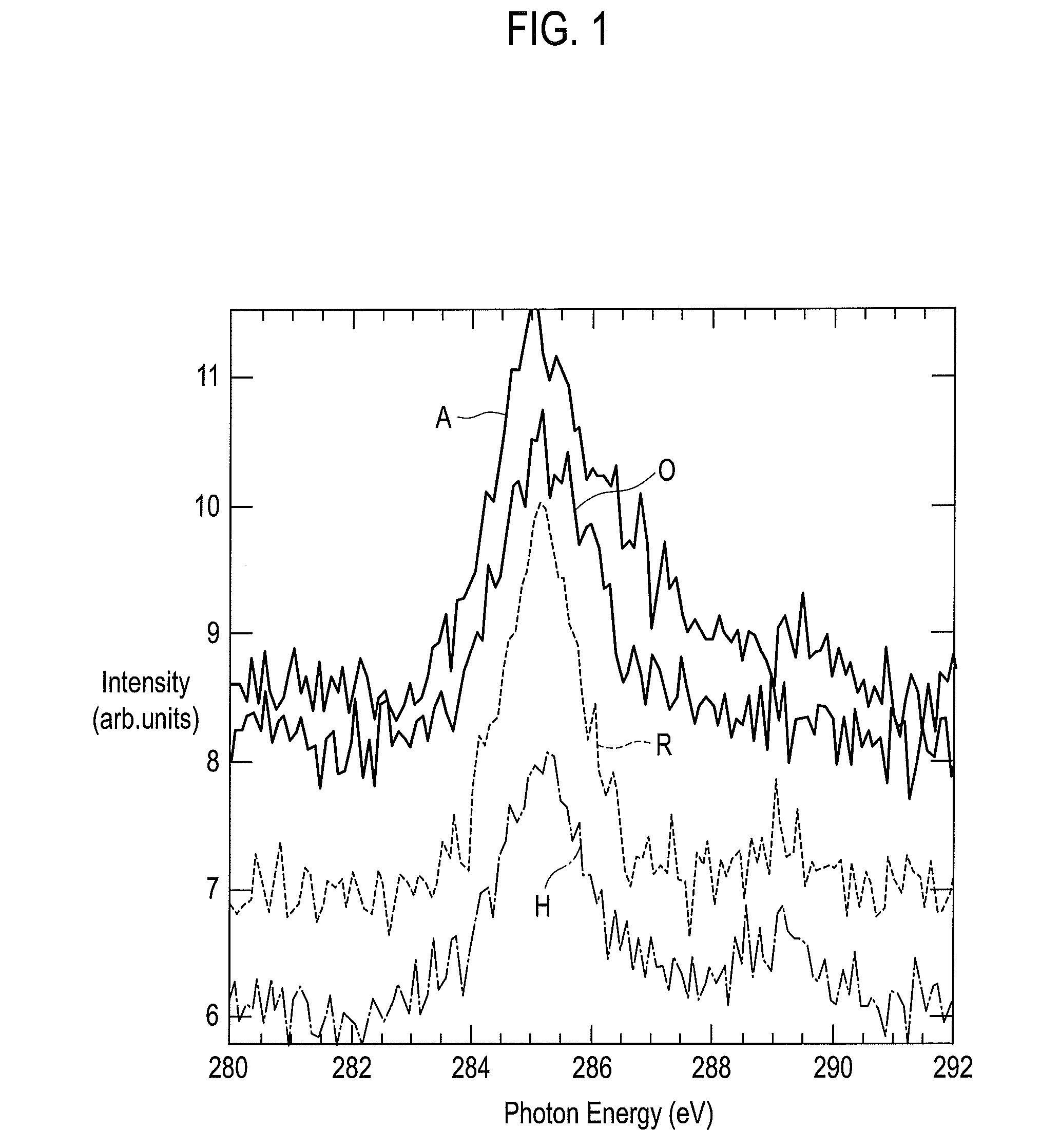
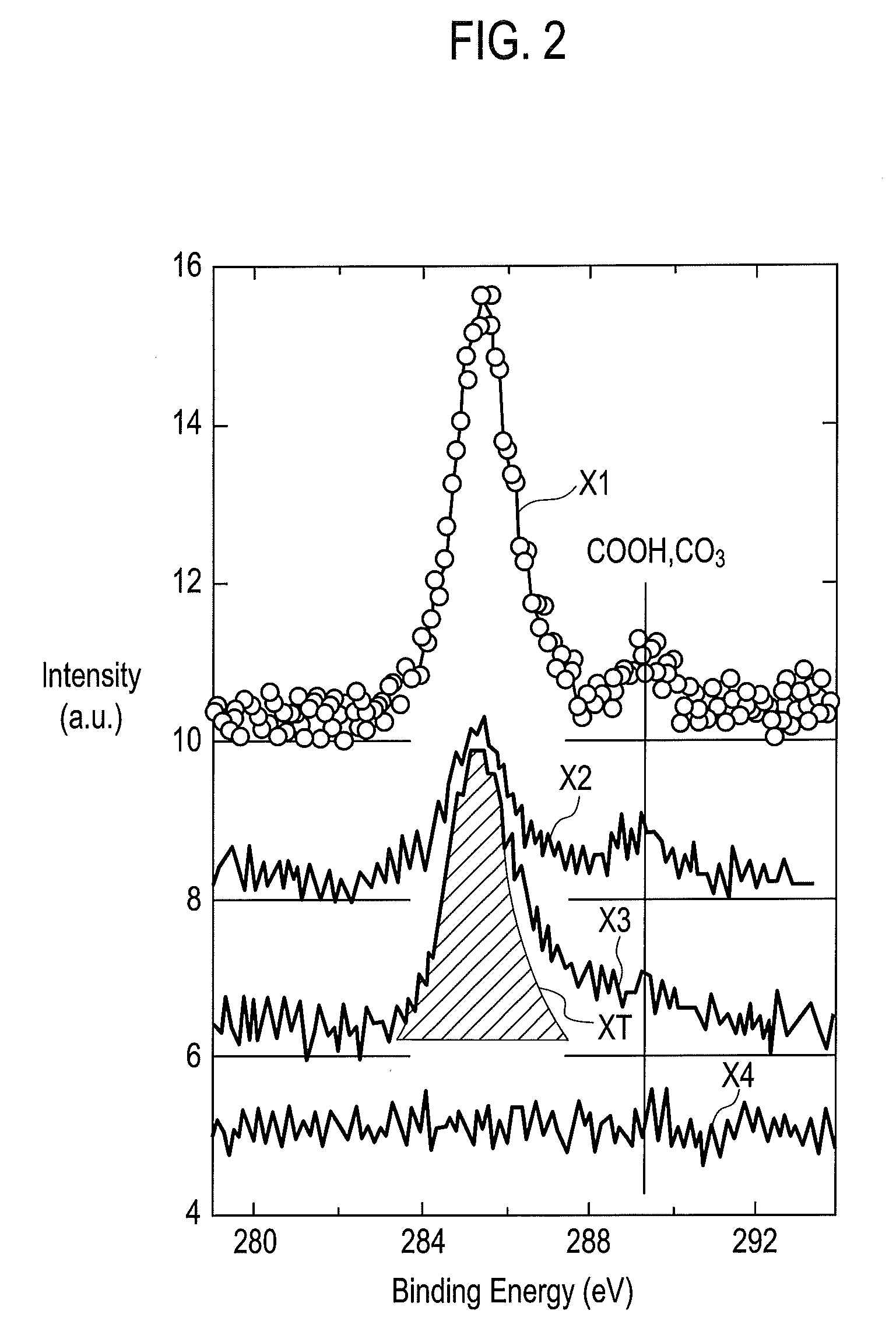
[0040]FIG. 6(b) is an image of the ZnO substrate surface where an abnormal diffraction pattern was measured in RHEED (reflection high energy electron diffraction) measurement. The image was captured in a field of view of 1 μm×1 μm using an AMF (...


PUM


Abstract

Provided are a ZnO-based substrate having a high-quality surface suitable for crystal growth, a method for processing the ZnO-based substrate, and a ZnO-based semiconductor device. The ZnO-based substrate is formed such that any one of a carboxyl group and a carbonate group is substantially absent in a principal surface on a crystal growth side. Also, in order for a carboxyl group or a carbonate group to be substantially absent, any one of oxygen radicals, oxygen plasma and ozone is brought into contact with the surface of the ZnO-based substrate before the crystal growth is started. Consequently, cleanness of the surface of the ZnO substrate is enhanced, thereby enabling fabrication of a high-quality ZnO-based thin film on the substrate.

Description

TECHNICAL FIELD[0001]The present invention relates to a ZnO-based substrate suitable for crystal growth of a ZnO-based thin film and the like, a method for processing the ZnO-based substrate, and a ZnO-based semiconductor device using these.BACKGROUND ART[0002]ZnO-based semiconductors have been expected to be applied to ultraviolet LEDs used as light sources for illuminations, backlights and the like, as well as to high-speed electronic devices, surface acoustic wave devices, and so forth. A ZnO-based semiconductor has drawn attention to its versatility, large light emission potential and the like. However, no significant development has been made on such a ZnO-based semiconductor as a semiconductor device material. The largest obstacle is that p-type ZnO cannot be obtained because of difficulty in acceptor doping.[0003]In recent years, however, as shown in Non-patent Documents 1 and 2, technological advancement has made it possible to obtain p-type ZnO and also to observe light emi...

Claims


Application Information

Patent Timeline
Patent Type & Authority Applications(United States)
IPC IPC(8): H01L29/22H01L21/36
CPCC30B33/12C30B29/16
Inventor NAKAHARA, KENAKASAKA, SHUNSUKEKAWASAKI, MASASHIOHTOMO, AKIRATSUKAZAKI, ATSUSHI
Owner ROHM CO LTD
Why Eureka
Try Eureka