White organic light-emitting device
- Summary
- Abstract
- Description
- Claims
- Application Information
AI Technical Summary
Benefits of technology
Problems solved by technology
Method used
Image
Examples
example 1
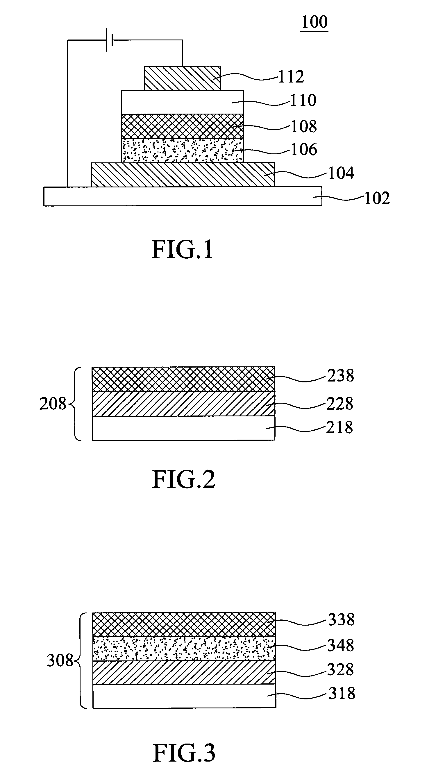
[0043]In Example 1, B1, B2, Y1 and Y2 comprised the following components:
[0044]B1: a host material (4CzPBP), a first transition metal organic complex (FIrpic) and a carrier transport material (TCTA) at a weight ratio of 75:15:10.
[0045]Y1: a host material (4CzPBP), a second transition metal complex (PO-01) and a carrier transport material (TCTA) at a weight ratio of 85:5:10.
[0046]Y2: a host material (PPT), a second transition metal complex (PO-01) and a carrier transport material (TCTA) at a weight ratio of 85:5:10.
[0047]B2: a host material (PPT), a first transition metal organic complex (FIrpic) and a carrier transport material (TCTA) at a weight ratio of 75:15:10.
[0048]The white organic light-emitting device of the present invention was fabricated according to the following procedure.
[0049]In the example, 150 nm-thick ITO was formed on a 0.7 mm-thick glass substrate as an anode. NPB having a thickness of 10 nm was coated on the anode to form a hole transport layer by thermal evapor...
example 2
[0052]In Example 2, B1, B2, Y1 and Y2 comprised the following components:
[0053]B1: a host material (4CzPBP), a first transition metal organic complex (FIrpic) and a carrier transport material (TCTA) at a weight ratio of 75:15:10.
[0054]Y1: a host material (4CzPBP) and a second transition metal complex (PO-01) at a weight ratio of 95:5.
[0055]Y2: a host material (PPT) and a second transition metal complex (PO-01) at a weight ratio of 95:5.
[0056]B2: a host material (PPT), a first transition metal organic complex (FIrpic) and a carrier transport material (TCTA) at a weight ratio of 75:15:10.
[0057]Moreover, the white organic light-emitting device in Example 2 was fabricated according to the procedure in Example 1.
[0058]In the example, a light-emitting multilayer B1-Y1-Y2-B2 was composed of four layers that emitted lights in the order of blue-yellow-yellow-blue lights, and Y1 and Y2 layers did not contain carrier transport materials. Test results of the current efficiency and operating vol...
example 3
[0059]In Example 3, B1, B2, and Y1 comprised the following components:
[0060]B1: a host material (4CzPBP), a first transition metal organic complex (FIrpic) and a carrier transport material (TCTA) at a weight ratio of 75:15:10.
[0061]Y1: a second transition metal complex.
[0062]B2: a host material (PPT), a first transition metal organic complex (FIrpic) and a carrier transport material (TCTA) at a weight ratio of 75:15:10.
[0063]Moreover, the white organic light-emitting device in example 3 was fabricated according to the procedure in example 1, wherein the thickness of Y1 layer was 0.1 nm. In the example, a light-emitting multilayer B1-Y1-B2 was composed of three layers that emitted lights in the order of blue-yellow-blue lights. Test results of the current efficiency and operating voltages of the device at luminance of 1000 cd / m2 and the color coordinates of white light of the device are shown in Table 2.
PUM
 Abstract
Description
Claims
Application Information


