

Spin transport device
- Summary
- Abstract
- Description
- Claims
- Application Information
AI Technical Summary
Benefits of technology
Problems solved by technology
Method used
Image

Examples
first embodiment
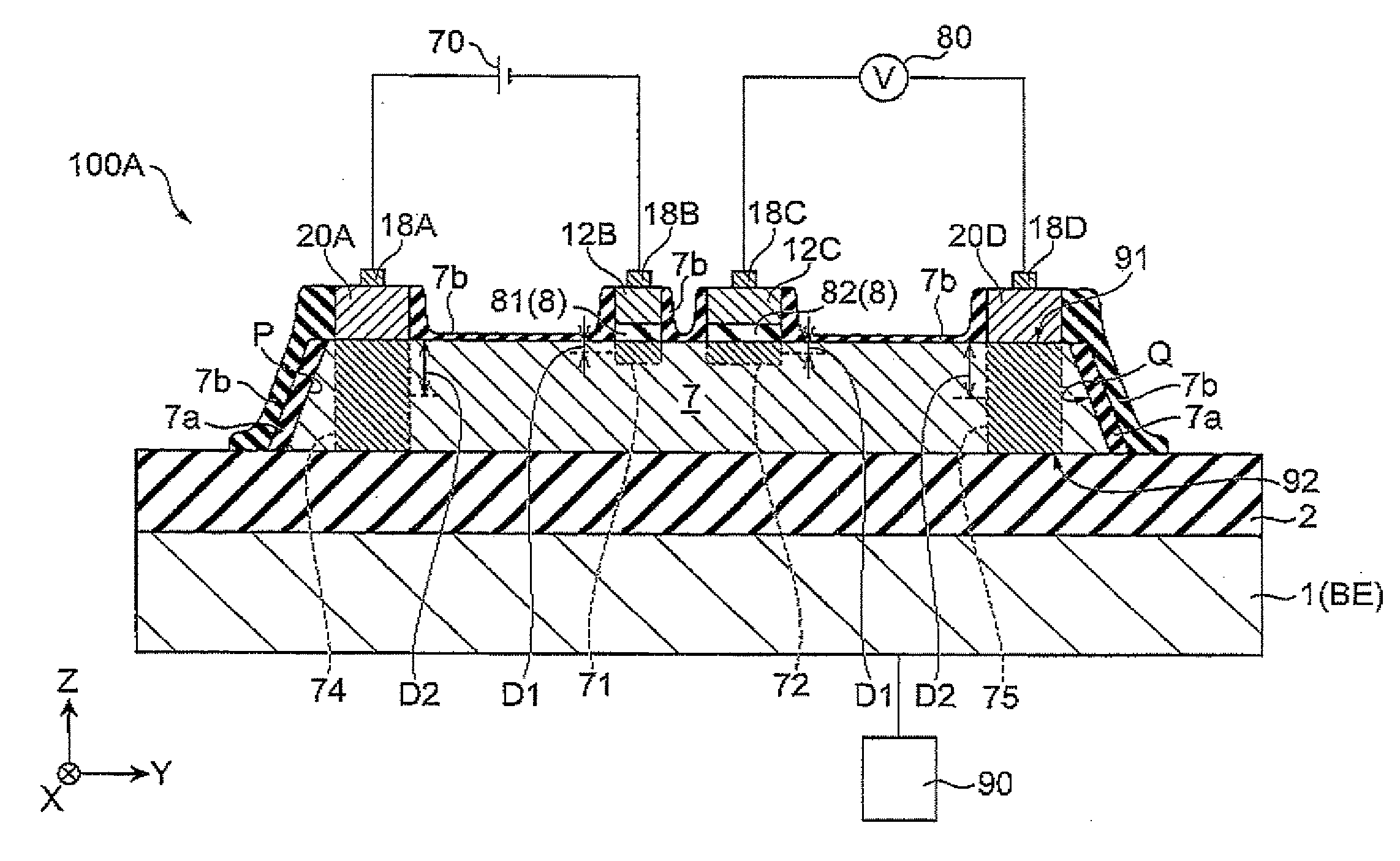
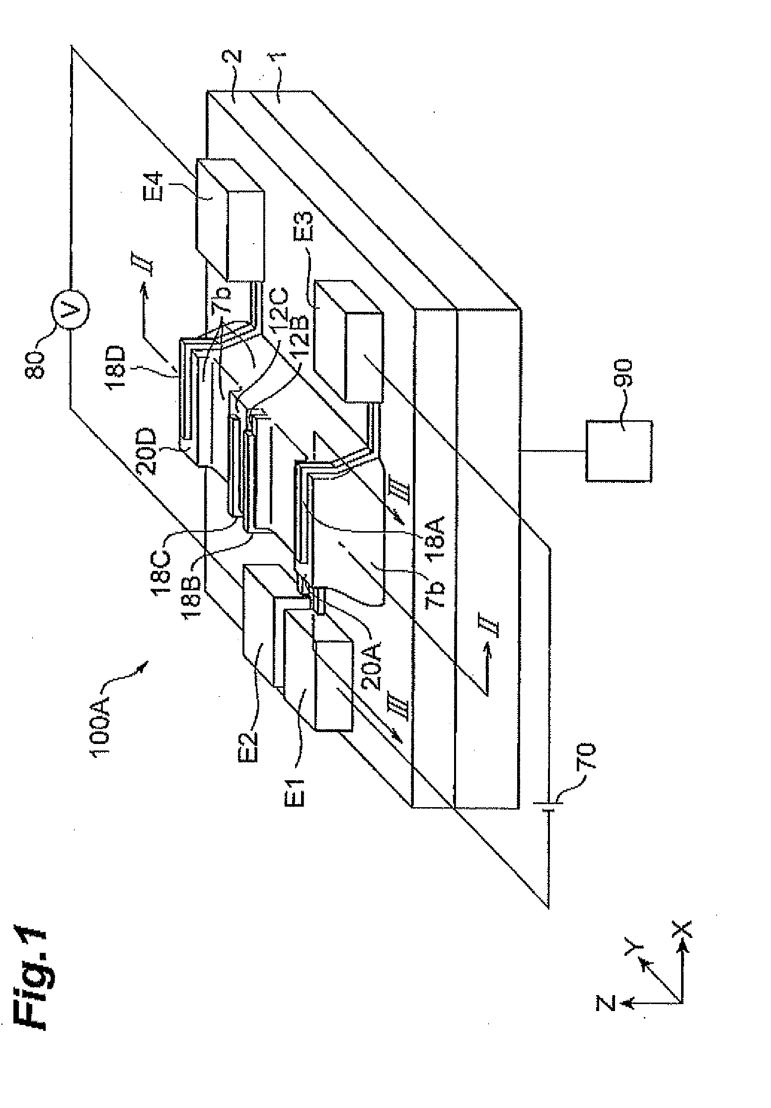
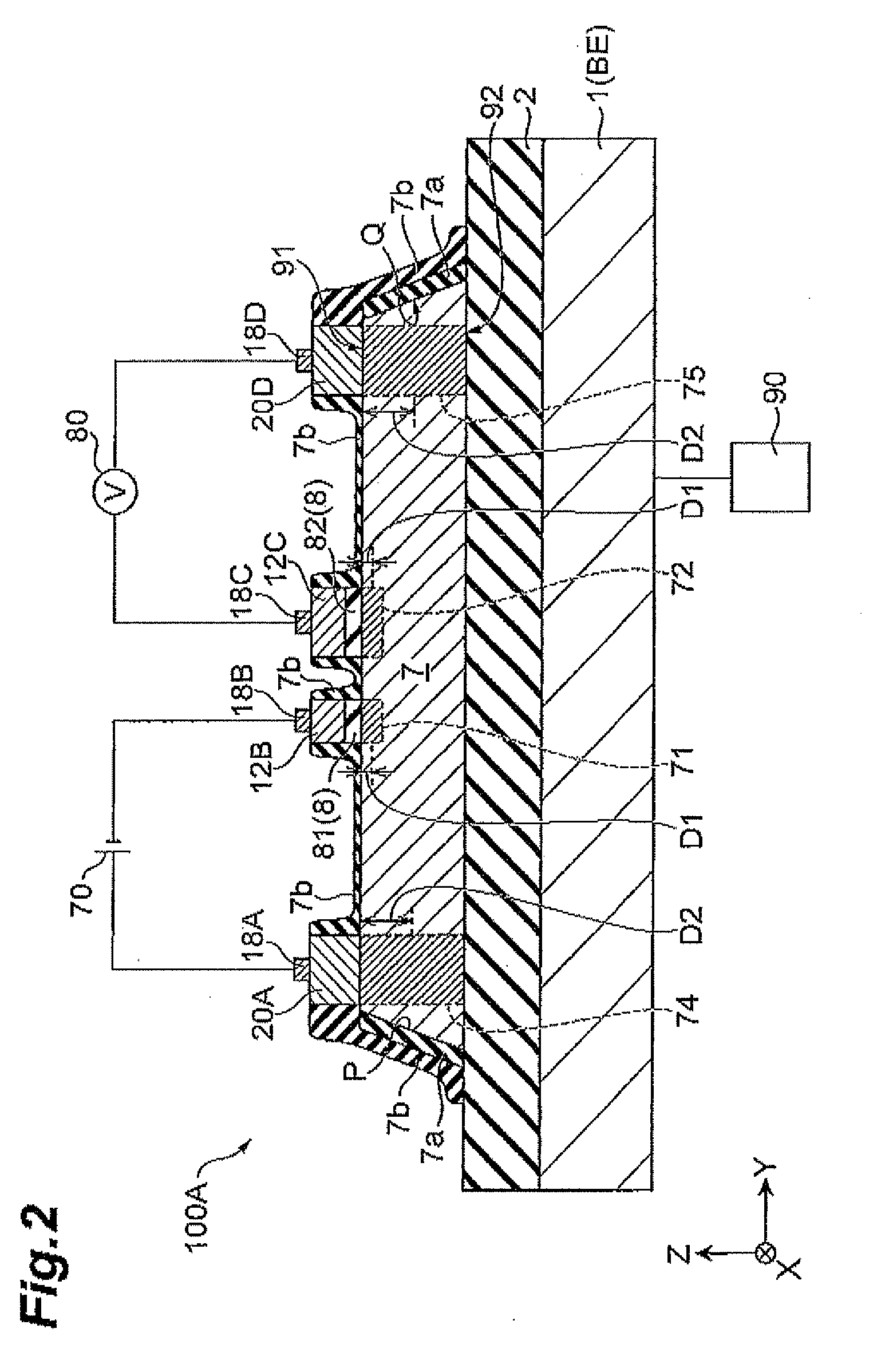
[0039]FIG. 1 is a perspective view of a spin transport device 100A. FIG. 2 is a sectional view taken along line II-II in FIG. 1, and FIG. 3 is a sectional view taken along line III-III in FIG. 1.
[0040]As illustrated in FIG. 2, a spin transport device 100A, in the case of using silicon as a semiconductor, mainly comprises a silicon substrate 1, a silicon oxide layer 2, a silicon channel 7, an insulating layer 8, a magnetization fixed layer 12B, a magnetization free layer 12C, a first electrode 20A and a second electrode 20D.
[0041]On the silicon substrate 1, the silicon oxide layer 2 and the silicon channel 7 are provided in this order. As the silicon substrate 1, the silicon oxide layer 2 and the silicon channel 7, for example, an SOI (Silicon On Insulator) substrate can be used.
[0042]The insulating layer 8 is an insulating film for using a tunnel magneto-resistance effect. The insulating layer 8 is provided on and in contact with the silicon channel 7. In an example as illustrated i...
second embodiment
[0071]In the second embodiment, a thin film magnetic recording / reproducing head 200 including a spin transport device 100C and a magnetic recording portion 100D will be described. FIG. 6 is a partial sectional view illustrating a thin film magnetic recording / reproducing head 200 according to the second embodiment, and FIG. 7 is a sectional view taken along line VI-VI in FIG. 6.
[0072]The thin film magnetic recording / reproducing head 200 performs a recording and reading operation of magnetic information in a position where its air bearing surface (medium opposite surface) S is arranged opposite to a recording surface 20a of a magnetic recording medium 20. The magnetic recording medium 20 includes a recording layer 20b having a recording surface 20a and a soft magnetic support layer 20c laminated on the recording layer 20b, and moves relative to the thin film magnetic recording / reproducing head 200 in a direction that is indicated as a Z direction in FIG. 6.
[0073]The spin transport dev...
example 2
[0110]An adhered material on the surface was removed by cleaning the AlTiC substrate. A NiFe layer was formed on the AlTiC substrate with a thickness of 50 nm. By milling the NiFe layer, a lower magnetic shield layer was obtained. A silicon oxide layer was formed on the NiFe layer with a thickness of 50 nm. A portion of the silicon oxide layer was milled up to the NiFe layer, and a Cu layer and an Al layer were filled. The surface of the silicon oxide layer and the Al layer was polished by a chemical mechanical polishing (CMP) method so that the surface became smooth. After the polishing, the Cu layer and the Al layer functioned as the first electrode. On the smoothed silicon oxide layer and Al layer, a polycrystalline silicon layer was formed. A silicon channel was obtained by changing the polycrystalline silicon layer to a single crystalline silicon layer using pulse irradiation of a carbon dioxide laser. The laser irradiation temperature was set to a temperature at which the poly...
PUM
 Abstract
Description
Claims
Application Information