

Method for Forming Nanotube Semiconductor Devices
- Summary
- Abstract
- Description
- Claims
- Application Information
AI Technical Summary
Benefits of technology
Problems solved by technology
Method used
Image

Examples
first embodiment
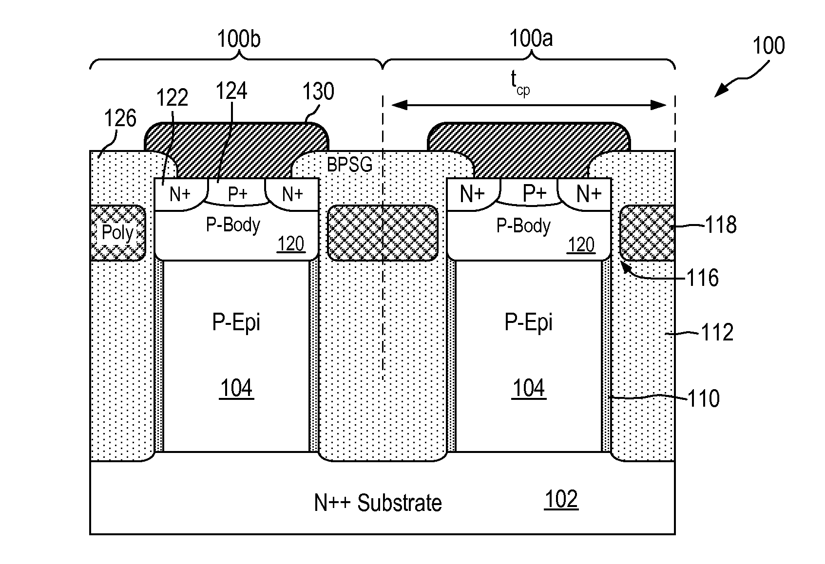
[0051]FIG. 1 is a cross-sectional view of a vertical trench MOSFET device according to the present invention. Referring to FIG. 1, an N-type vertical trench MOSFET device (“NMOS transistor”) 100 is formed in an array of parallely connected transistor cells 101a and 101b. A desired number of transistor cells are used to form the array to realize an NMOS transistor 100 having the desired breakdown voltage and Rdson (drain-to-source “On” resistance) characteristic. The transistor array can be a 1-dimensional or 2-dimensional array depending on the number of transistor cells involved. For instance, a stripe cell structure can be used for a 1-dimensional array and a hexagonal cell structure can be used for a 2-dimensional array, as will be described in more detail below.
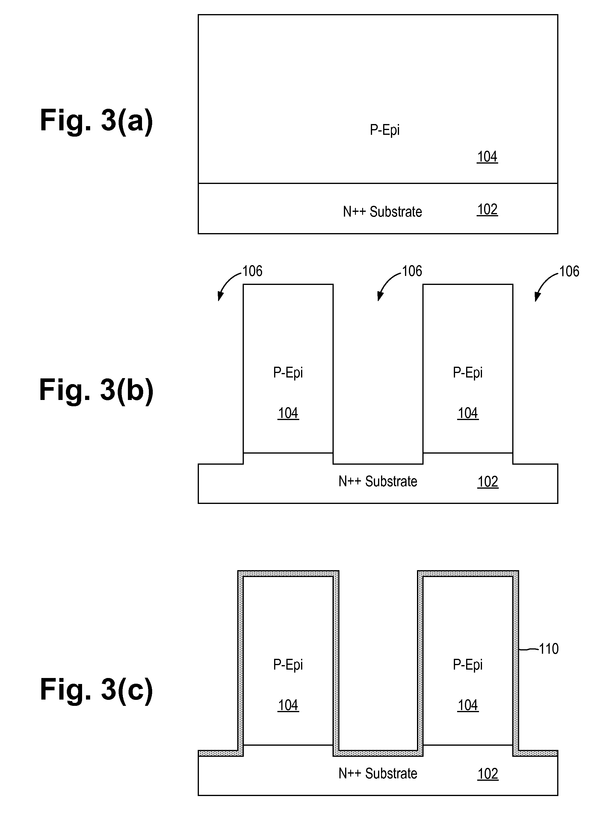
[0052]NMOS transistor 100 is formed on a very heavily doped N++ substrate 102. N++ substrate 102 serves as the drain electrode of the transistor. Oxide-filled trenches 112 are formed in a P-type epitaxial (P-Mesa-Epi) lay...
second embodiment
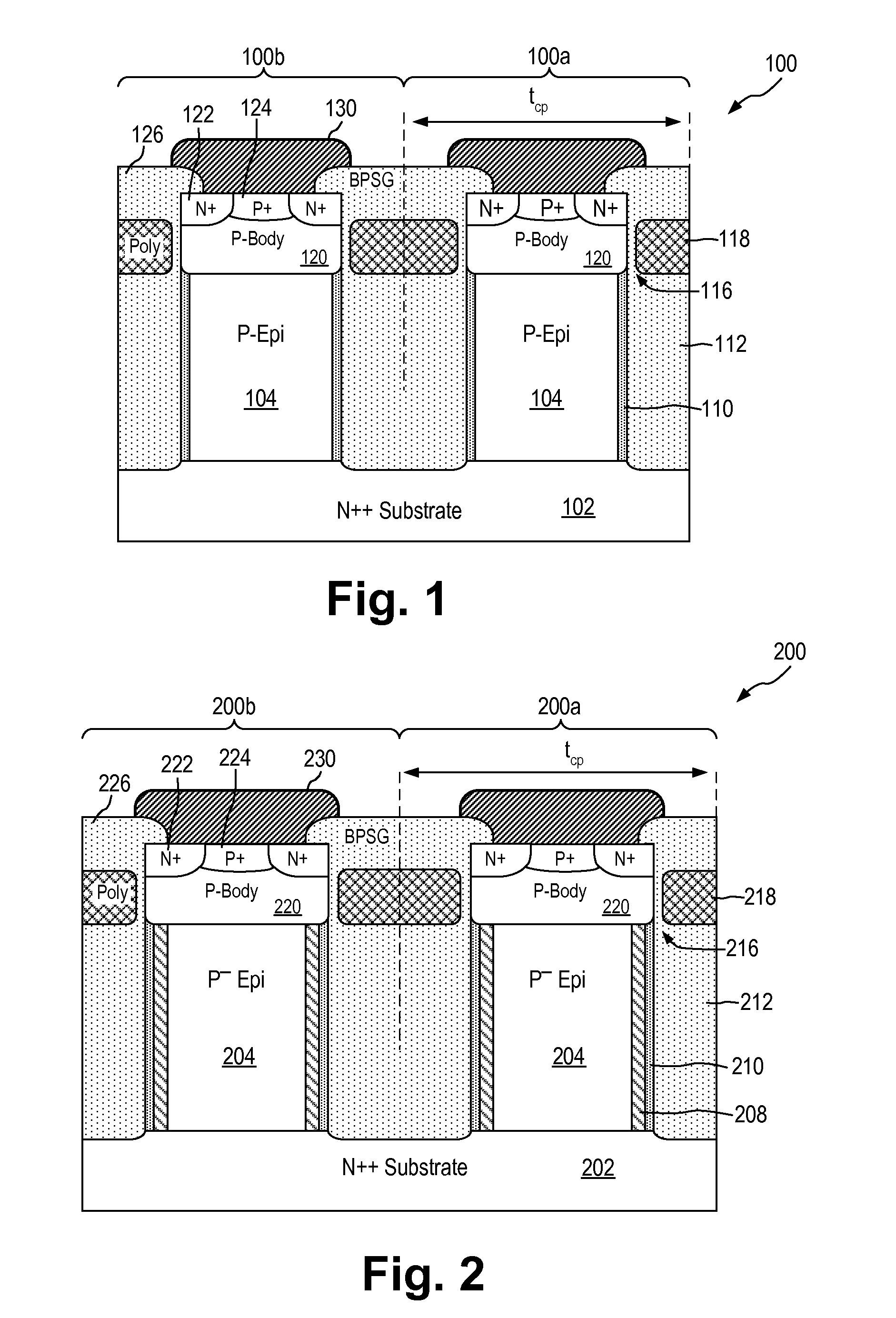
[0064]FIG. 2 is a cross-sectional view of a vertical trench MOSFET device according to the present invention. Referring to FIG. 2, an N-type vertical trench MOSFET device (“NMOS transistor”) 200 is formed in an array of parallely connected transistor cells 201a and 201b. A desired number of transistor cells are used to form the array to realize an NMOS transistor 200 having the desired breakdown voltage characteristic. The transistor array can be a 1-dimensional or 2-dimensional array depending on the number of transistor cells involved.
[0065]NMOS transistor 200 has the same structure as NMOS transistor 100 of FIG. 1 except for an additional thin P-type epitaxial (P-Epi) layer 208 formed adjacent to the thin N-Epi layer 210. The N-Epi layer 210 and P-Epi layer 208 forming a “double nanotube” structure. Furthermore, the P-type epitaxial layer 204 in which the transistor cells are formed is very lightly doped P-type epitaxial layer, denoted “P-Mesa Epi” in FIG. 2. The thin P-Epi layer...
PUM
 Abstract
Description
Claims
Application Information