Heat Shield for Heater in Semiconductor Processing Apparatus

a technology of semiconductor processing and heat shield, which is applied in the direction of vacuum evaporation coating, electrolysis components, coatings, etc., can solve the problems of significant reduction of undesired depositions on chamber components, including stems and pedestals, and fluorine molecules that are far less effective in active cleaning (etching) to achieve the effect of improving the efficiency of the apparatus

Active Publication Date: 2010-12-16
NOVELLUS SYSTEMS
View PDF11 Cites 60 Cited by
  • Summary
  • Abstract
  • Description
  • Claims
  • Application Information

AI Technical Summary

Benefits of technology

[0008]According to this invention, a novel approach is employed in a semiconductor processing apparatus where a high performance heat shield is employed in conjunction with a heater and workpiece platen assembly where the heat shield insulation has low conductivity over a wide range of temperatures so that a significant amount of heat is redirected from the heat shield back to the heater to heat up the workpiece. As a result, a substantial savings in heater power consumption is achieved since the power required to heat the workpiece to a given temperature is now significantly reduced. Tests have shown that a reduction in power consumption of about 20% or more is achieved with a heater in semiconductor processing apparatus utilizing the high performance heat shield of this disclosure.

Problems solved by technology

In a film deposit processing apparatus, the amount of undesired depositions on chamber components, including the stem and pedestal, is significantly reduced because temperature levels required for deposition via gas-entrained constituents is deterred beyond the second side of the high performance heat shield, i.e., the side opposite to that in thermal communication with the heater body, since the temperature is not sufficiently high to readily permit a film deposition process.
However, as these cleaning species move toward the bottom of the chamber, the fluorine atoms readily combine into fluorine molecules that are far less effective in active cleaning (etching).

Method used


Image

  • Heat Shield for Heater in Semiconductor Processing Apparatus
  • Heat Shield for Heater in Semiconductor Processing Apparatus
  • Heat Shield for Heater in Semiconductor Processing Apparatus

Examples


Embodiment Construction

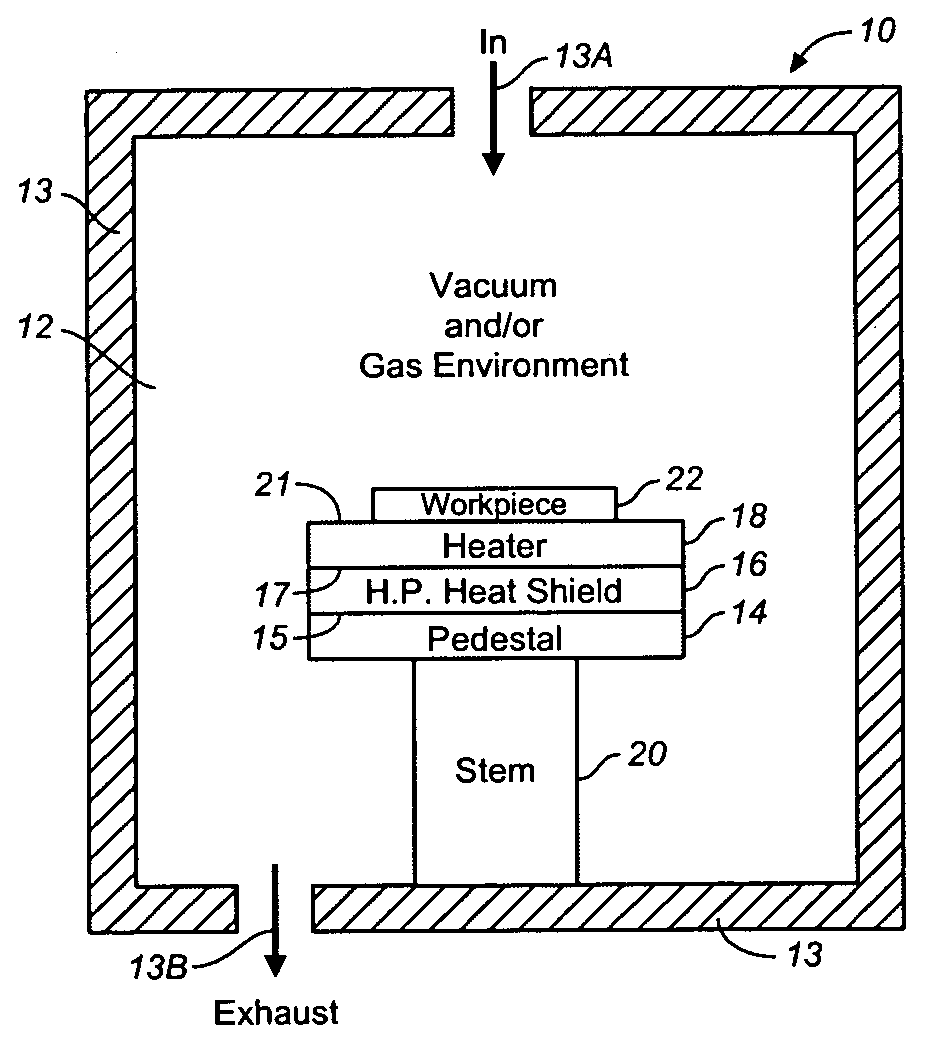
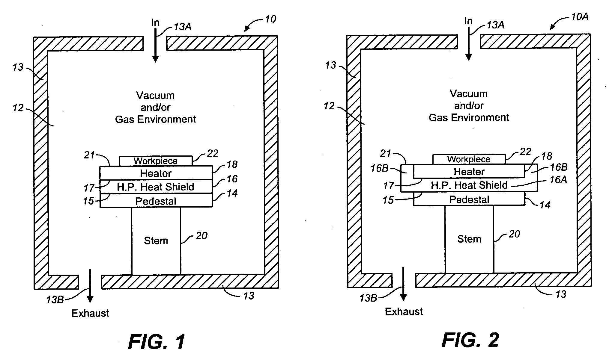
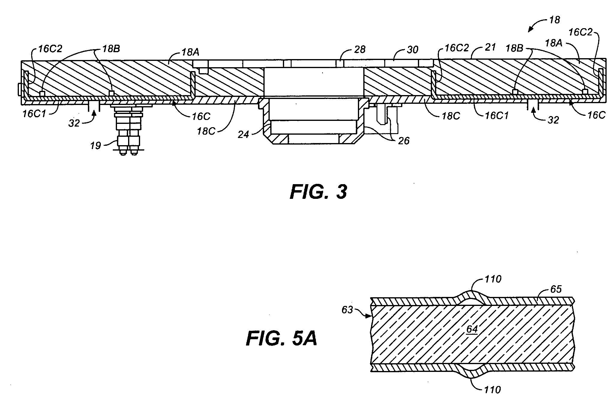
[0027]In the following description, for purpose of explanation, specific details are set forth in order to provide an understanding of the present invention. The present invention may, however, be practiced without some or all of these details. The embodiment of the present invention described below may be incorporated into a number of different electrical components, circuits, devices, and systems. Structures and devices shown in block diagram are illustrative of exemplary embodiments of the present invention and are not to be used as a pretext by which to obscure broad teachings of the present invention. Connections between components within the figures are not intended to be limited to direct connections. Rather, connections between components may be modified, re-formatted, or otherwise changed by intermediary components.

[0028]Reference in the specification to “one embodiment” or to “an embodiment” means that a particular feature, structure, characteristic, or function described ...


PUM

PropertyMeasurementUnit
temperatureaaaaaaaaaa
temperaturesaaaaaaaaaa

Abstract

A heat shield employed in semiconductor processing apparatus comprises a high performance insulation that has low thermal conductivity, such as, below the thermal conductivity of still air over a wide range of temperatures utilized in operation of the apparatus. As an example, the thermal conductivity of the insulation may be in the range of about 0.004 W / m·h to about 0.4 W / m·h over a temperature range of about 0° C. to about 600° C. or more. The deployment of the high performance heat shield reduces the power consumption necessary for the heater by as much as 20% to reach a desired processing temperature as compared to a case of heater power consumption required to reach the same desired temperature without the shield. Further, the heat shield significantly reduces the amount of undesired depositions from gas-entrained constituents on components in the chamber of the apparatus, particularly below or beyond the heat shield, by as much as 90% since the temperature drop is as much as ten orders of magnitude difference.

Description

BACKGROUND[0001]A. Technical Field[0002]The present invention relates generally to semiconductor processing and semiconductor processing apparatus and more particularly to improvements in the efficiency in the use and operation of semiconductor processing apparatus.[0003]B. Background of the Invention[0004]There is an initiated and ongoing trend in the development of semiconductor processing apparatus, particularly to improve their efficiency of operation and operate more “green” with less detrimental effects on the environment. That trend includes steps of going more “green” in the operation of such apparatus, such as, reducing the power consumption of the apparatus and reducing the required time and the amount of expense necessary to clean the apparatus between production runs. Examples of such apparatus are the heat treatment and deposition of various kinds of materials and / or layers on a workpiece, which may be a semiconductor wafer or any other type, and kind of substrate to be...

Claims


Application Information

Patent Timeline
Patent Type & Authority Applications(United States)
IPC IPC(8): H01L21/30C23C16/44C23C14/34C23C16/513H05K13/00
CPCY10T29/49002C23C16/4581C23C16/4586C23C16/4401H01L21/67103H01L21/68714
Inventor LIND, GARYOSTROWSKI, JOHN FLOYD
Owner NOVELLUS SYSTEMS
Why Eureka
Try Eureka