

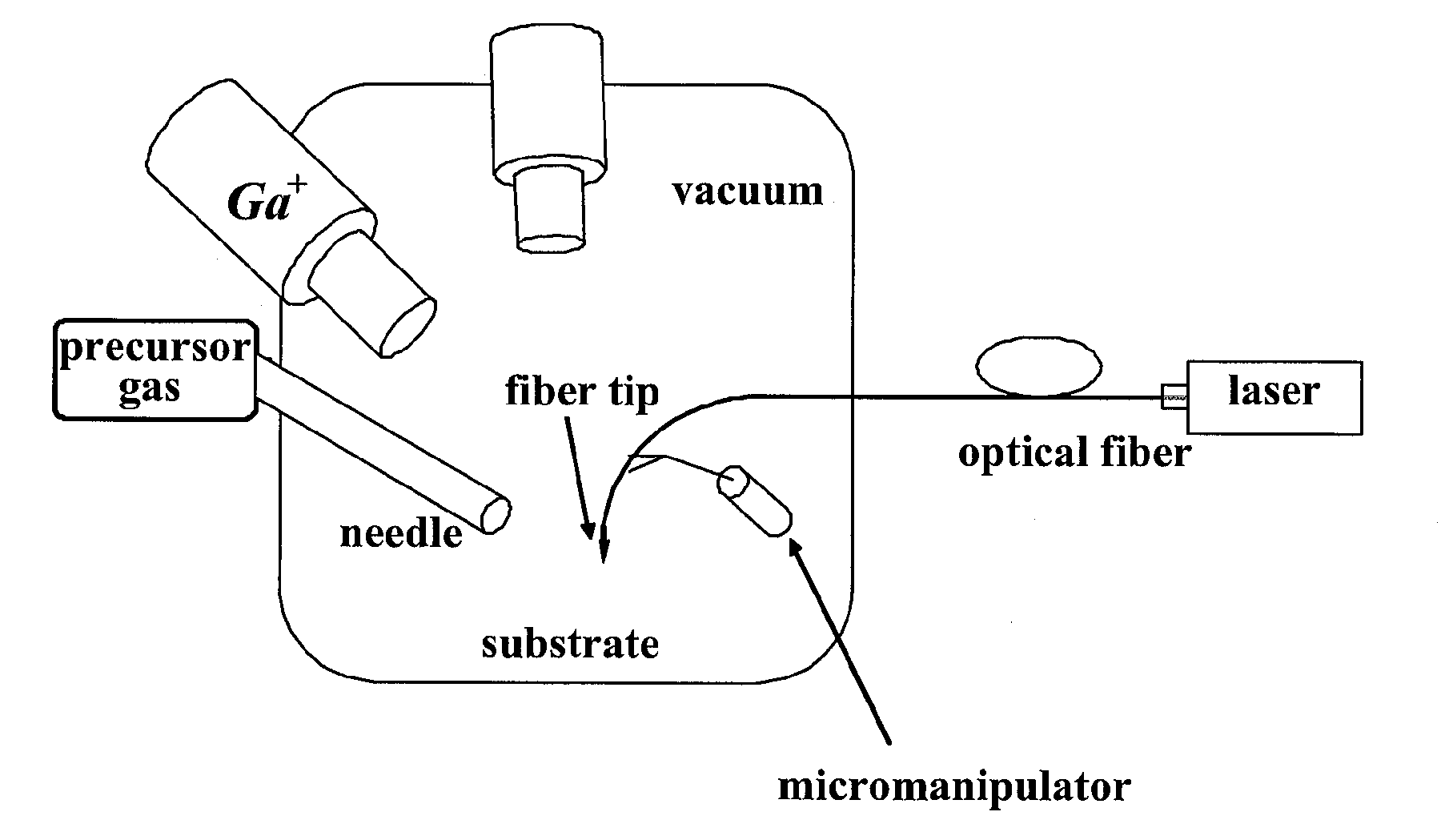
Laser-assisted nanomaterial deposition, nanomanufacturing, in situ monitoring and associated apparatus
a technology of laser-assisted nanomaterials and nano-manufacturing, which is applied in the direction of optical radiation measurement, solid state diffusion coating, chemical vapor deposition coating, etc., can solve the problems of inconvenient operation, high manufacturing cost, and limited minimum feature size of these methods
- Summary
- Abstract
- Description
- Claims
- Application Information
AI Technical Summary
Benefits of technology
Problems solved by technology
Method used
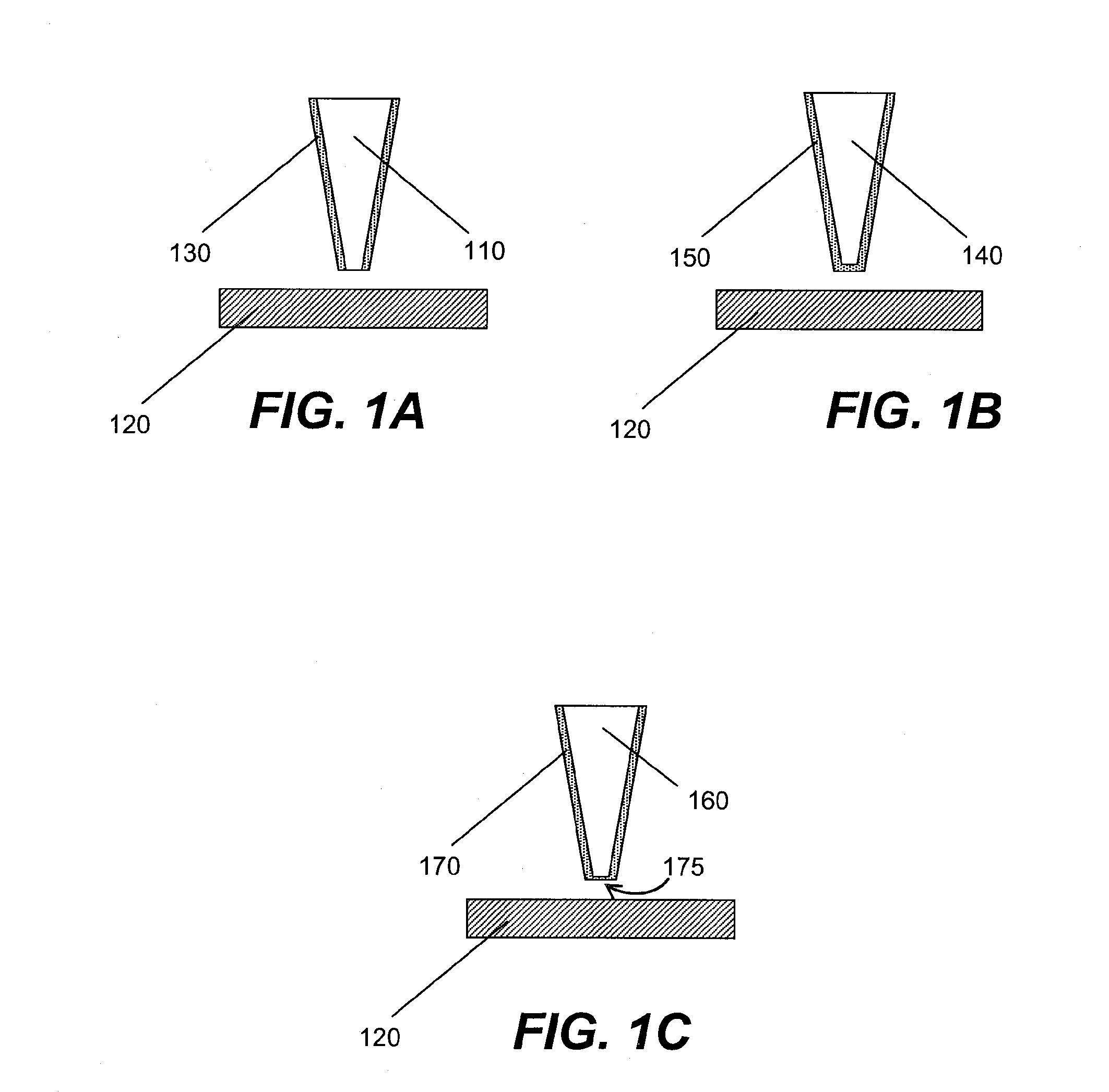
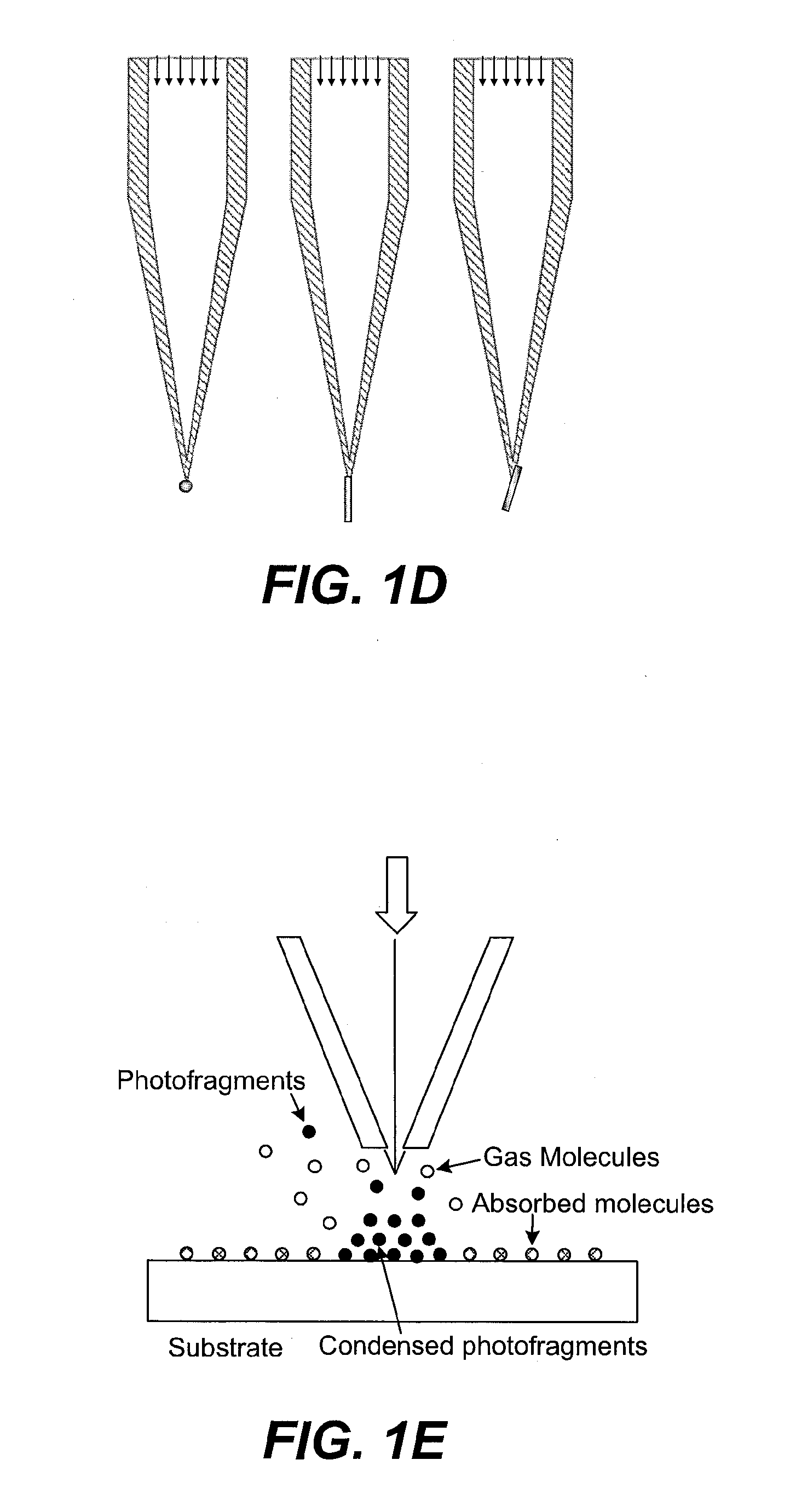
Image

Examples
example 1
In Situ Monitoring of Ablation Crater Fabrication
[0105]FIG. 10 shows in situ monitoring of fiber probe based ablation craters. Single nanosecond laser pulses of about 4-6 ns temporal pulse width and 532 nm wavelength were applied onto a silicon sample to fabricate each crater.
example 2
In Situ Cleaning of Agglomerated Nanoparticles
[0106]FIG. 11 shows the in situ cleaning of agglomerated nanoparticles (mixed polystyrene spheres of about 90 nm and about 300 nm diameters seen in panel (a)) by fiber probe illumination. A single nanosecond laser pulse of about 4-6 ns temporal pulse width, about 214 nJ pulse energy, and 532 nm wavelength was applied to remove particles from a silicon substrate (panel (b)).
example 3
Local Modification of Single Silicon Nanowires
[0107]FIG. 12 records the fiber probe based local modification of single silicon nanowires. Nanosecond laser pulses of about 4-6 ns temporal pulse width, 532 nm wavelength, and repetition rate of 10 Hz were applied to induce local modification. Laser pulse energy roughly one third of in situ measured bulk silicon substrate damage threshold value was used. FIGS. 12a and 12b show the nanowire damage after about 100 laser shots (12a), and after an additional about 100 laser shots (12b). FIG. 12c depicts an in situ magnified image of FIG. 12b.
PUM
| Property | Measurement | Unit |
|---|---|---|
| size | aaaaa | aaaaa |
| feature size | aaaaa | aaaaa |
| width | aaaaa | aaaaa |
Abstract
Description
Claims
Application Information