Method for manufacturing liquid crystal display device

a liquid crystal display and liquid crystal technology, applied in the field of liquid crystal display devices, can solve the problems of reduced viscosity of sealant, liquid crystal layer with stable blue phase cannot be formed, liquid crystal material might be irradiated, etc., and achieve the effect of increasing the width of sealant and improving adhesion

Active Publication Date: 2010-12-30
SEMICON ENERGY LAB CO LTD
View PDF28 Cites 24 Cited by
  • Summary
  • Abstract
  • Description
  • Claims
  • Application Information

AI Technical Summary

Benefits of technology

[0022]According to another embodiment of the disclosed invention, a photocurable and thermosetting second sealant is formed on an outer side than a thermosetting first sealant and made to serve for improvement of adhesion between substrates, whereby irradiation with ultraviolet rays for pre-curing the second sealant is not needed. Accordingly, a liquid crystal display device including a liquid crystal layer which exhibits a stable blue phase can be manufactured. Moreover, even in the case where polymer stabilization treatment is performed before the photocurable and thermosetting second sealant is irradiated with ultraviolet rays, when a thermosetting sealant is used as the first sealant which is in contact with the liquid crystal layer and the phot

Problems solved by technology

Therefore, there is a problem in that a liquid crystal layer which exhibits a stable blue phase cannot be formed.
In addition, at this time, even in the case where a light shielding mask is formed to prevent the liquid crystal material from being irradiated with ultraviolet rays, there is a concern that the liquid crystal material might be irradiated with light reflected from wirings formed over a substrate and the like.
On th

Method used


Image

  • Method for manufacturing liquid crystal display device
  • Method for manufacturing liquid crystal display device
  • Method for manufacturing liquid crystal display device

Examples


embodiment 1

[0039]In this embodiment, an example of a method for manufacturing a liquid crystal display device is described with reference to drawings.

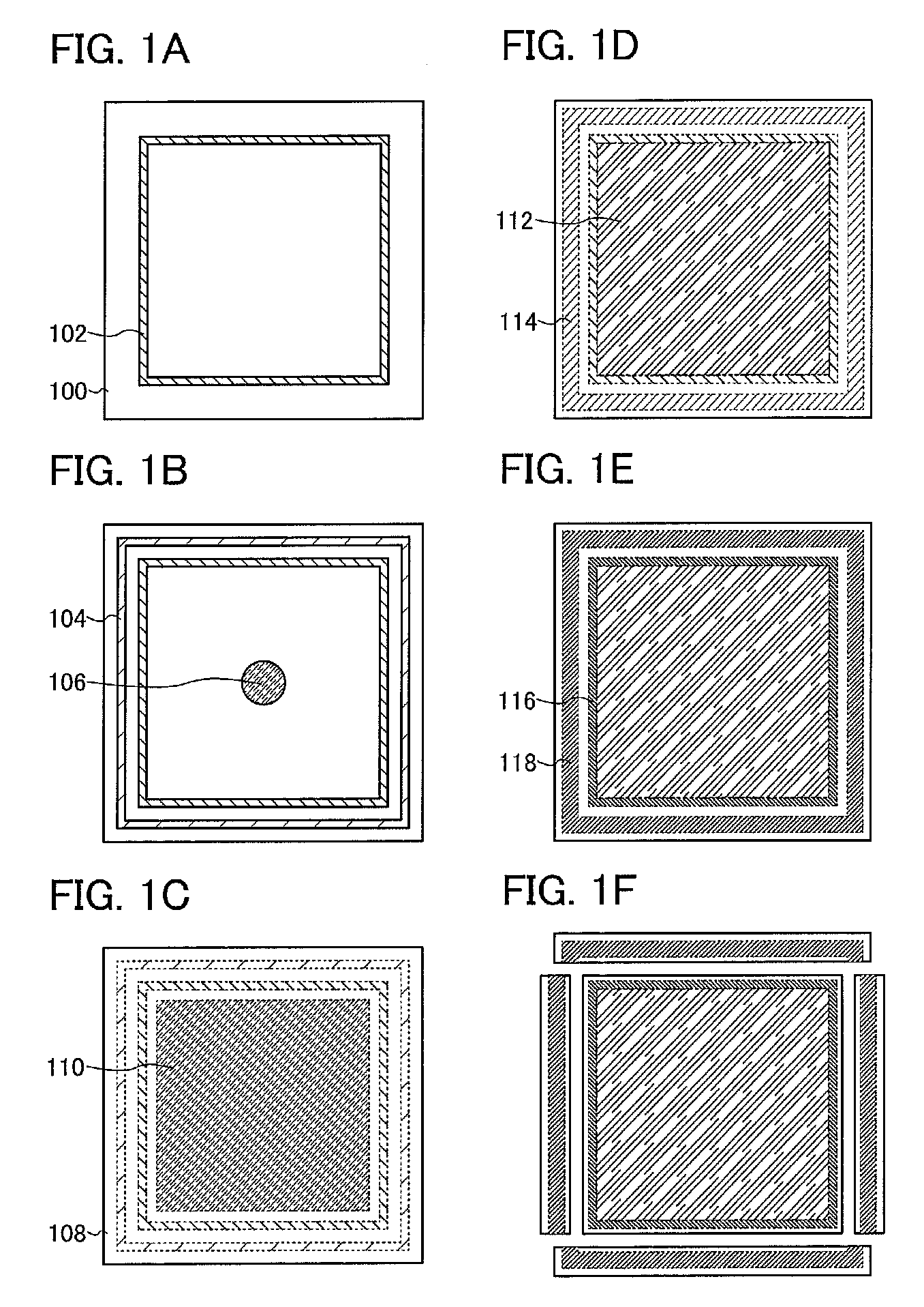
[0040]First, a first substrate 100 is prepared, and a first sealant 102 is formed over the first substrate 100 (see FIG. 1A).

[0041]As the first substrate 100, glass substrates used for electronics industry (also called a “non-alkali glass substrate”) such as an aluminosilicate glass substrate, an aluminoborosilicate glass substrate, or a barium borosilicate glass substrate; a quartz substrate; a ceramic substrate; a plastic substrate; or the like can be used. An element such as a transistor for forming a pixel and the like of a liquid crystal display device may be provided over the substrate.

[0042]The first sealant 102 can be formed using a thermosetting resin. The thermosetting resin is a resin cured by heat treatment. For the thermosetting resin, an epoxy-based resin, an acrylate-based (urethane acrylate) resin, or the like can be used. A fille...

modified example

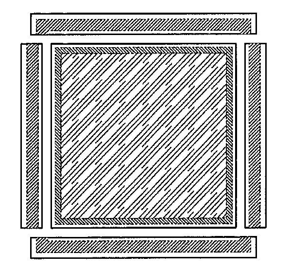
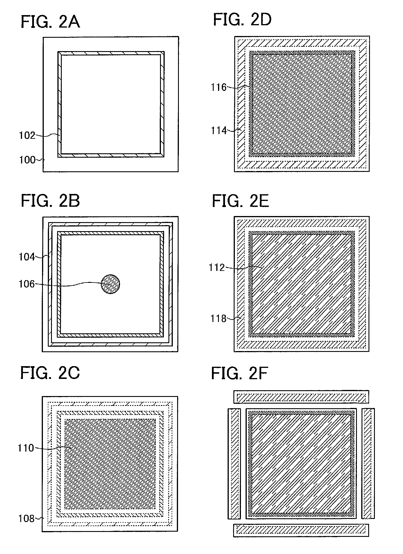
[0070]FIGS. 1A to 1F illustrate a case where the first sealant 102 is post-cured after polymer stabilization treatment; however, this embodiment is not limited to such a manner. For example, as illustrated in FIGS. 2A to 2F, the second substrate 108 and the first substrate 100 provided with the first sealant 102 may be attached to each other, the second sealant 104, and the liquid crystal material 106 (see FIGS. 2A to 2C), and then heat treatment may be performed to post-cure the first sealant 102 (see FIG. 2D). After that, polymer stabilization treatment may be performed (see FIG. 2E). That is, FIGS. 2A to 2F illustrate a case where the order of the step in FIG. 1D is replaced with the order of the step in FIG. 1E in the steps illustrated in FIGS. 1A to 1F.

[0071]Note that FIGS. 2A to 2F illustrate a case where the substrates are cut after polymer stabilization treatment (see FIG. 2F); however, the substrates may be cut in a period after the first sealant 102 is post-cured and befor...

embodiment 2

[0076]In this embodiment, a method for manufacturing liquid crystal display devices, which is different from the method in Embodiment 1, is described with reference to drawings. Specifically, a step of taking out a plurality of panels (obtaining a plurality of panels) from one panel is described. Note that the manufacturing method described in this embodiment has a lot in common with those in FIGS. 1A to 1F and FIGS. 2A to 2F. Therefore, description of common portions is omitted and different portions are described below.

[0077]First, the first substrate 100 is prepared and a plurality of first sealants 102a, 102b, 102c, and 102d is formed over the first substrate 100 (see FIG. 3A).

[0078]The first sealants 102a to 102d can be formed using a thermosetting sealant. The description of the first sealant 102 in Embodiment 1 can be referred to for details of materials used for the first sealants 102a to 102d and the like; therefore, the description thereof is omitted here.

[0079]Further, af...


PUM

PropertyMeasurementUnit
Temperatureaaaaaaaaaa
Phase transition temperatureaaaaaaaaaa
Temperatureaaaaaaaaaa

Abstract

It is an object to provide a method for manufacturing a liquid crystal display device including a liquid crystal layer which exhibits a stable blue phase. The following steps are performed: a first step of forming a thermosetting first sealant so as to form a frame over a first substrate; a second step of forming a photocurable and thermosetting second sealant on an outer side than the first sealant over the first substrate; a third step of dropping a liquid crystal material which exhibits a blue phase at a given temperature on an inner side than the first sealant; a fourth step of attaching a second substrate to the first substrate in a reduced-pressure atmosphere; a fifth step of performing polymer stabilization treatment on the liquid crystal material; and a sixth step of curing the first sealant through heat treatment.

Description

BACKGROUND OF THE INVENTION[0001]1. Field of the Invention[0002]The present invention relates to a liquid crystal display device and a method for manufacturing the liquid crystal display device.[0003]2. Description of the Related Art[0004]In recent years, display devices (flat panel display) which are very thin and lightweight as compared to cathode-ray tube display devices have developed. The flat panel displays include liquid crystal display devices which have liquid crystal elements, electro-luminescent (EL) display devices which have self-light emitting elements such as EL elements, plasma displays, and the like, and they are in competition in the market.[0005]Although each kind of flat panel display has good points and bad points as of now, the liquid crystal display devices are inferior to the other flat panel displays in the response time of an element (the speed of switching the display). Various techniques for overcoming the disadvantage in the response time have been propo...

Claims


Application Information

Patent Timeline
IPC IPC(8): B32B37/14B32B38/00B32B38/10
CPCG02F1/1339G02F1/1341Y10T156/1052G02F2001/13793G02F2001/13415G02F1/13415G02F1/13793C09K2003/1062G02F1/1334G02F1/13394
Inventor ISHITANI, TETSUJIKUBOTA, DAISUKETAMURA, TOMOHIRO
Owner SEMICON ENERGY LAB CO LTD
Why Eureka
Try Eureka