Nitride semiconductor chip, method of fabrication thereof, and semiconductor device

a technology semiconductor device, which is applied in the direction of semiconductor devices, basic electric elements, electrical apparatus, etc., can solve the problems of significantly reducing luminous efficacy, simultaneous polarization in the active layer, and increased lattice distortion, so as to facilitate the acquisition of nitride semiconductor chip, enhance luminous efficacy, and improve el emission pattern

Inactive Publication Date: 2011-01-06
SHARP KK
View PDF31 Cites 22 Cited by
  • Summary
  • Abstract
  • Description
  • Claims
  • Application Information

AI Technical Summary

Benefits of technology

[0067]As described above, according to the invention, it is possible to easily obtain a nitride semiconductor chip that offers enhanced luminous efficacy as a result of an improved EL emission pattern, a method of its manufacture, and a semiconductor device incorporating such a nitride semiconductor chip.
[0068]Moreover, according to the invention, it is possible to easily obtain a nitride semiconductor chip that has good

Problems solved by technology

Inconveniently, however, the c plane of a GaN substrate is a polar plane having polarity in the c-axis direction, and therefore stacking nitride semiconductor layers including an active layer on the c plane inconveniently causes spontaneous polarization in the active layer.
Also inconveniently, when nitride semiconductor layers including an active layer are stacked on the c plane, as the In composition ratio increases, lattice distortion increases, inducing in the active layer a strong internal electric field due to piezoelectric polarization.
Accordingly, increasing the In composition ratio in an attempt to realize light emission in a green region suffers from the problem that, as the emission wavelength is lengthened, luminous efficacy significantly lowers.
As discussed above, it has been found out that, in nitride semiconductor light-emitting chips using a nitride semiconductor substrate having the m plane as the principal growth plane, as distinct from nitride semiconductor light-emitting chips using the c plane, whereas the lowering of luminous effi

Method used


Image

  • Nitride semiconductor chip, method of fabrication thereof, and semiconductor device
  • Nitride semiconductor chip, method of fabrication thereof, and semiconductor device
  • Nitride semiconductor chip, method of fabrication thereof, and semiconductor device

Examples


embodiment 1

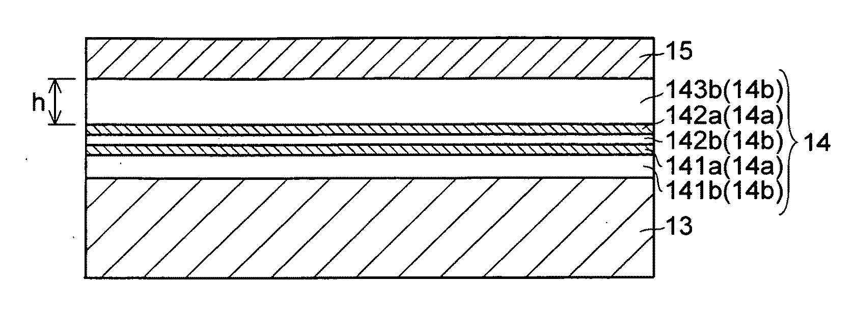
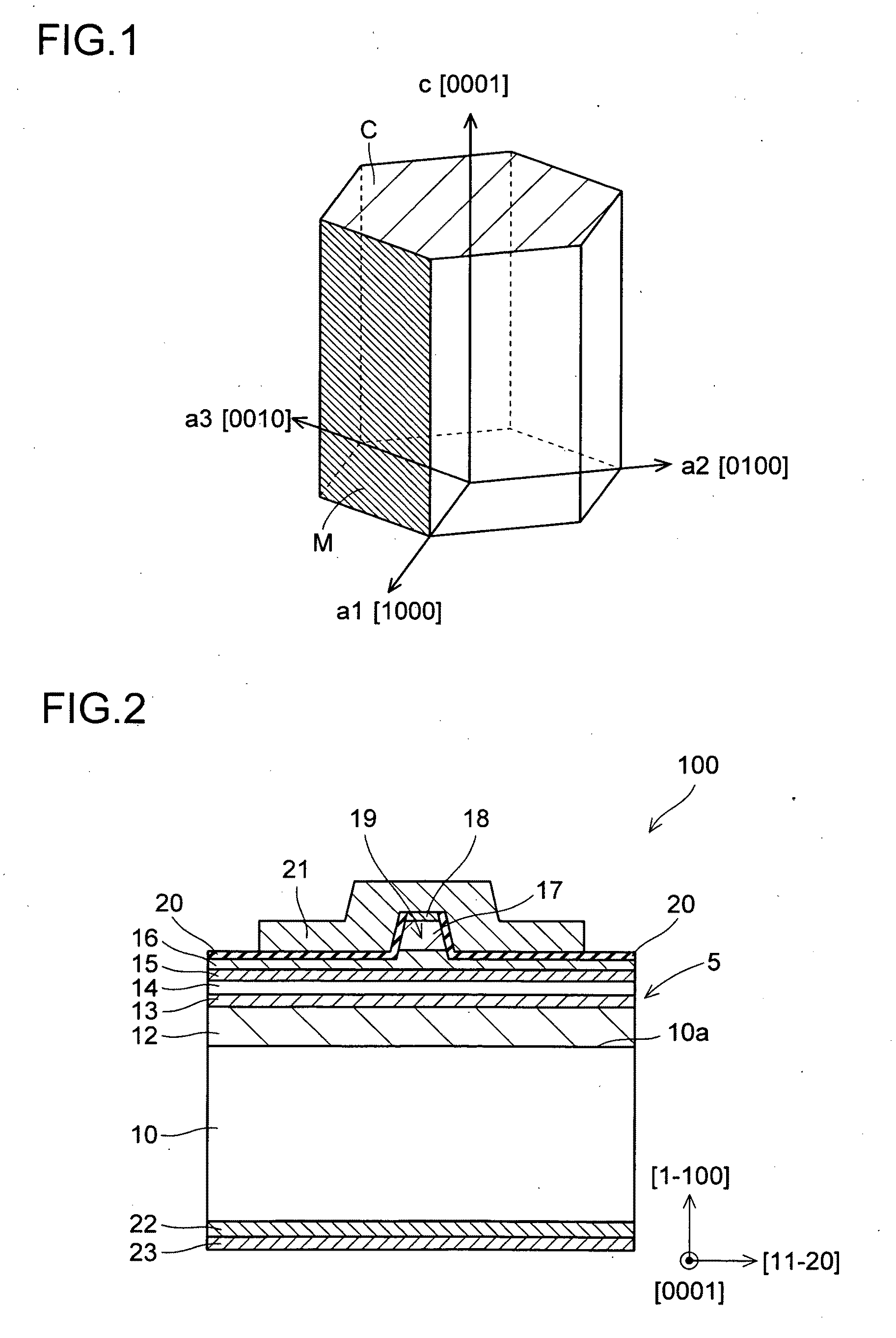
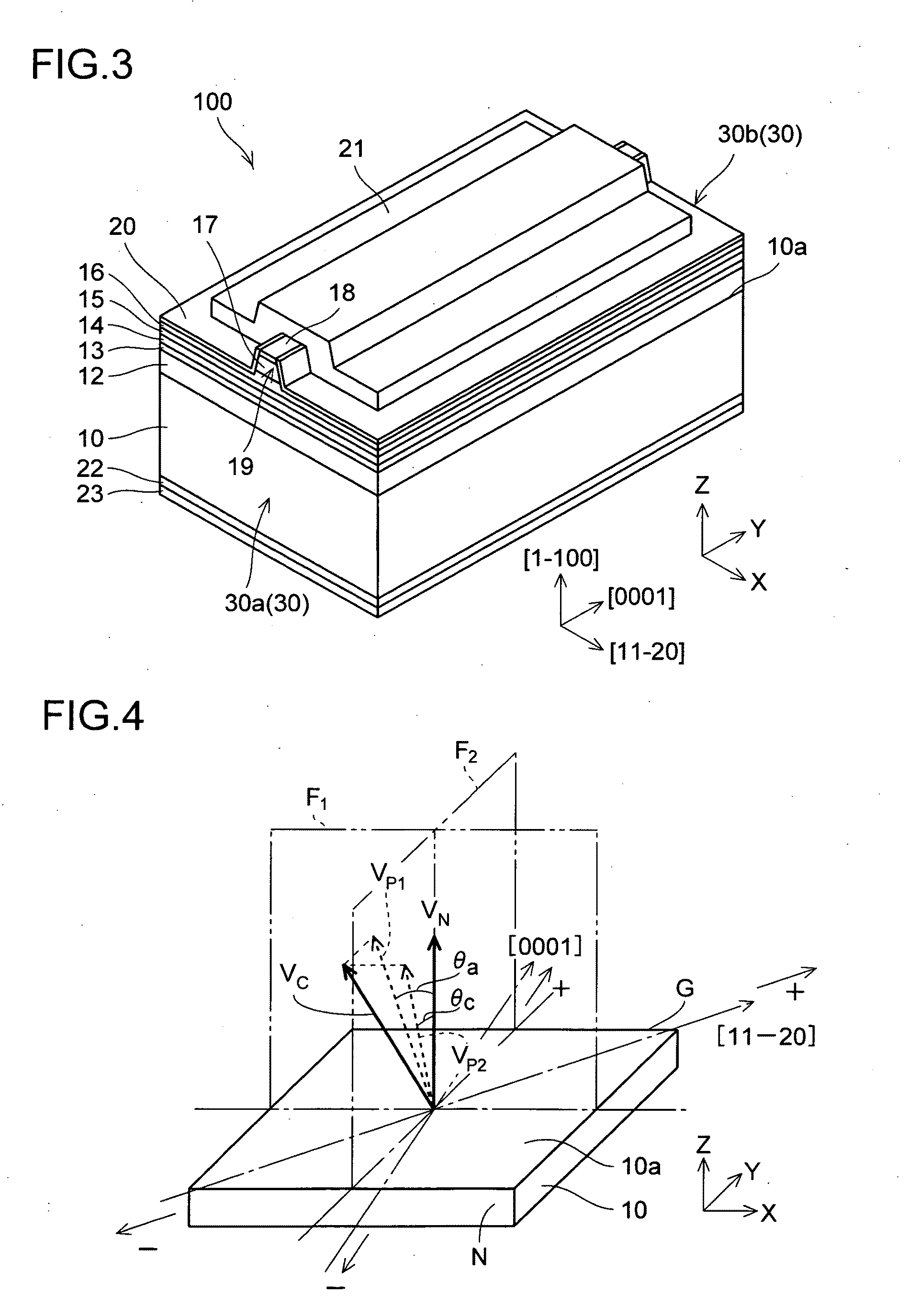
[0161]FIG. 1 is a schematic diagram illustrating a crystal structure of a nitride semiconductor. FIG. 2 is a sectional view showing the structure of a nitride semiconductor laser chip according to a first embodiment (Embodiment 1) of the invention. FIG. 3 is an overall perspective view of a nitride semiconductor laser chip according to Embodiment 1 of the invention. FIGS. 4 to 6 are diagrams illustrating the structure of a nitride semiconductor laser chip according to Embodiment 1 of the invention. First, with reference to FIGS. 1 to 6, the structure of a nitride semiconductor laser chip 100 according to Embodiment 1 of the invention will be described.

[0162]The nitride semiconductor laser chip 100 according to Embodiment 1 is formed of a nitride semiconductor having a crystal structure of a hexagonal crystal system as shown in FIG. 1. In this crystal structure, when the hexagonal crystal system is considered to be a hexagonal column about a c axis [0001], the plane (the top face C o...

example 1

Practical Example 1

[0224]As a nitride semiconductor laser chip according to Practical Example 1, a nitride semiconductor laser chip similar to the one according to Embodiment 1 described above was fabricated by use of a GaN substrate having an off-angle of 1.7 degrees in the a-axis direction and an off-angle of +0.1 degrees in the c-axis direction relative to the m plane {1-100}. In other respects, the structure of Practical Example 1 was similar to that of Embodiment 1 described above. Another nitride semiconductor laser chip fabricated in a similar manner to the one according to Embodiment 1 described above but by using a GaN substrate having no off-angle (an m-plane just substrate) was taken as Comparative Example 1. In other respects, the structure of the nitride semiconductor laser chip of Comparison Example 1 was similar to that of Embodiment 1.

[0225]With respect to Practical Example 1 and Comparison Example 1, the threshold current was measured. Whereas with the nitride semic...

embodiment 2

[0226]FIG. 23 is a sectional view showing the structure of a nitride semiconductor laser chip according to a second embodiment (Embodiment 2) of the invention. FIG. 24 is an overall perspective view of the nitride semiconductor laser chip according to Embodiment 2 of the invention. FIGS. 25 and 26 are diagrams illustrating the structure of the nitride semiconductor laser chip according to Embodiment 2 of the invention. Next, with reference to FIGS. 23 to 26, the structure of the nitride semiconductor laser chip 1100 according to Embodiment 2 of the invention will be described.

[0227]As shown in FIGS. 23 and 24, the nitride semiconductor laser chip 1100 according to Embodiment 2 is formed by use of a GaN substrate 10 similar to that in Embodiment 1 described previously, and has a plurality of nitride semiconductor layers stacked on the principal growth plane 10a of the GaN substrate 10. That is, in Embodiment 2, as in Embodiment 1 described previously, on the principal growth plane 10...


PUM


Abstract

A nitride semiconductor chip is provided that offers enhanced luminous efficacy and an increased yield as a result of an improved EL emission pattern and improved surface morphology (flatness). This nitride semiconductor laser chip (nitride semiconductor chip) includes a GaN substrate having a principal growth plane and individual nitride semiconductor layers formed on the principal growth plane of the GaN substrate. The principal growth plane is a plane having an off angle in the a-axis direction relative to the m plane, and the individual nitride semiconductor layers include a lower clad layer of AlGaN. This lower clad layer is formed in contact with the principal growth plane of the GaN substrate.

Description

[0001]This nonprovisional application claims priority under 35 U.S.C. §119(a) on Patent Application No. 2009-158199 filed in Japan on Jul. 2, 2009 and Patent Application No. 2009-170472 filed in Japan on Jul. 21, 2009, the entire contents of which are hereby incorporated by reference.BACKGROUND OF THE INVENTION[0002]1. Field of the Invention[0003]The present invention relates to a nitride semiconductor chip, to a method of manufacture thereof, and to a semiconductor device. More particularly, the present invention relates to a nitride semiconductor chip provided with a nitride semiconductor substrate, to a method of manufacture thereof, and to a semiconductor device incorporating such a nitride semiconductor chip.[0004]2. Description of Related Art[0005]Nitride semiconductors as exemplified by GaN, AlN, InN, and their mixed crystals are characterized by having wider band gaps Eg than AlGaInAs- and AlGaInP-based semiconductors and in addition being direct band gap materials. For thes...

Claims


Application Information

Patent Timeline
IPC IPC(8): H01L29/205H01L21/20H01L29/20
CPCH01L21/02389H01L21/0243H01L21/0262H01L21/0254H01L21/02433
Inventor KAMIKAWA, TAKESHIOHTA, MASATAKA
Owner SHARP KK
Why Eureka
Try Eureka