Ultraviolet light emitting diode/laser diode with nested superlattice

a light-emitting diode and ultra-violet technology, applied in the direction of lasers, semiconductor devices, semiconductor lasers, etc., can solve the problems of crystalline defects, difficult manufacturing, and thermal mismatch between iii-nitride lattice and other problems, to achieve the effect of reducing the propagation of defects and significantly facilitating strain managemen

Active Publication Date: 2011-01-27
NIITEK
View PDF2 Cites 41 Cited by
  • Summary
  • Abstract
  • Description
  • Claims
  • Application Information

AI Technical Summary

Benefits of technology

[0013]The present invention is an ultra-violet light-emitting device and method for fabricating an ultraviolet light emitting device. In a preferred embodiment, the present invention is a deep ultra-violet light-emitting structure (λPeak=190-369 nm) with a nested superlattice. The ultraviolet light-emitting structure...

Problems solved by technology

These LEDs are difficult to manufacture for a number of reasons.
For example, defects arise from lattice and thermal mismatch between the group III-Nitride based semiconductor layers and a substrate such as sapphire, silicon carbide, or silicon on which they are constructed.
In addition, impurities and tilt boundaries result in the formation of crystalline defects.
These defects have been shown to reduce the efficiency and lifetime of LEDs and LDs fabricated from these materials.
This method, however, has been shown to be ineffective for the growth of aluminum-containing III-Nitride based semiconductors because of the tendency for the aluminum to stick to the masked material and disrupt the lateral overgrowth.
All of these techniques suffer from the same limitation as the ELOG approach for aluminum containing III-Nitri...

Method used


Image

  • Ultraviolet light emitting diode/laser diode with nested superlattice
  • Ultraviolet light emitting diode/laser diode with nested superlattice
  • Ultraviolet light emitting diode/laser diode with nested superlattice

Examples


Embodiment Construction

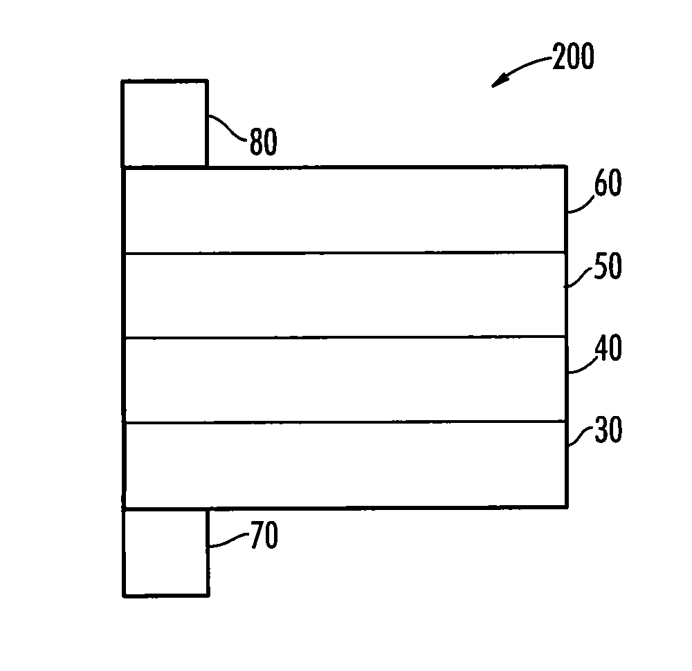
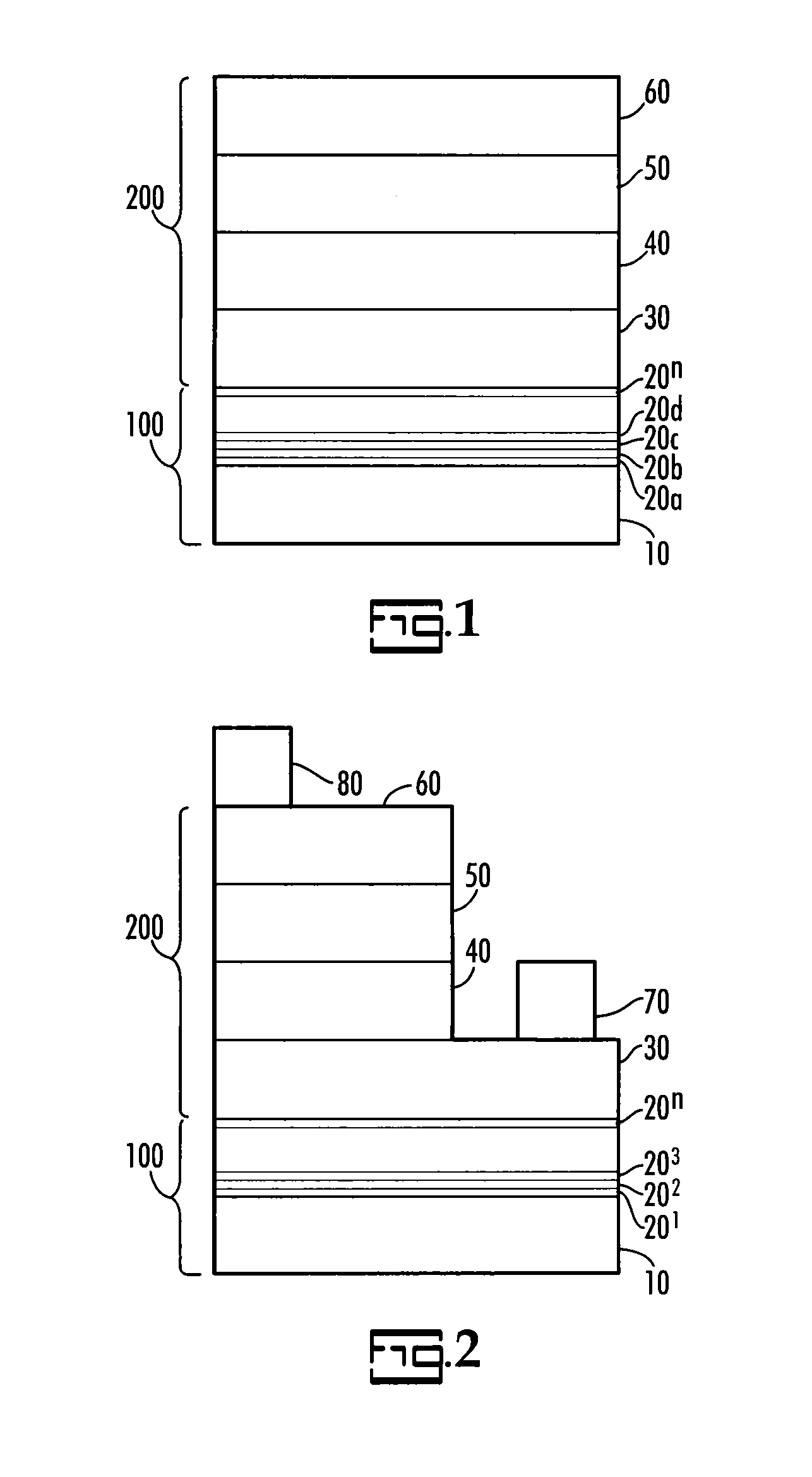
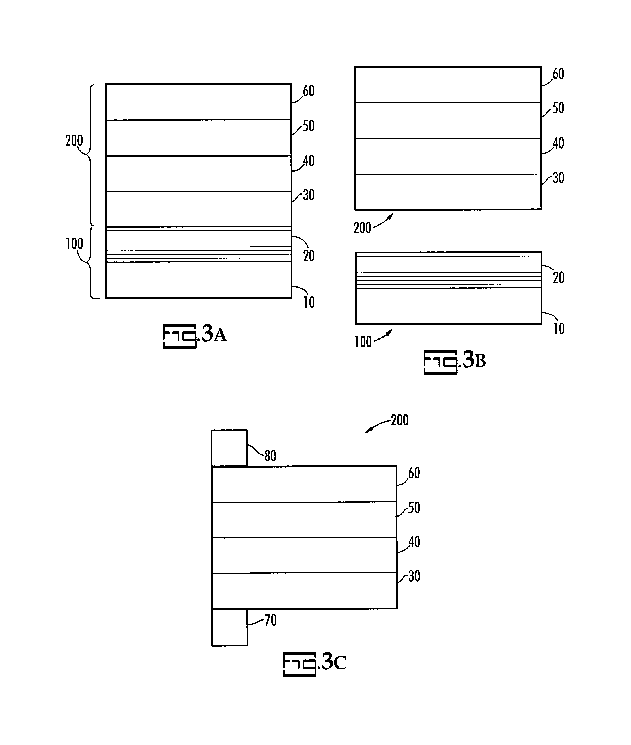
[0025]The present invention is directed to a light-emitting device (LED) and a method for making an LED, particularly, one that emits deep ultraviolet light. In particular, it is directed to an improved template with a nested superlattice wherein strain and propagation of dislocations is mitigated by the nested superlattice. The template serves as a platform for the ultraviolet light-emitting structure.

[0026]The invention will be described with reference to the various figures forming an integral part of the instant disclosure. The figures, and descriptions thereof, refer specifically to preferred embodiments without limit thereto. Throughout the figures similar elements will be numbered accordingly.

[0027]An embodiment of the invention will be described with reference to FIG. 1 wherein a schematic cross-sectional view is provided. In FIG. 1, a template, 100, includes a substrate, 10, upon which subsequent layers are grown.

[0028]The nested superlattice forms a transitional compositio...


PUM


Abstract

A light emitting device with a template comprising a substrate and a nested superlattice. The superlattice has Al1-x-yInyGaxN wherein 0≦x≦α and 0≦y≦1 with x increasing with distance from said substrate. An ultraviolet light-emitting structure on the template has a first layer with a first conductivity comprising Al1-x-yInyGaxN wherein α≦x; a light emitting quantum well region above the first layer comprising Al1-x-yInyGaxN wherein α≦x≦b; and a second layer over the light emitting quantum well with a second conductivity comprising Al1-x-yInyGaxN wherein b≦x. The light emitting device also has a first electrical contact in electrical connection with the first layer, a second electrical contact in electrical connection with the second layer; and the device emits ultraviolet light.

Description

CROSS-REFERENCE TO RELATED APPLICATIONS [0001]The present invention claims priority to pending U.S. Provisional Patent Application No. 61 / 070,977 filed Mar. 27, 2008.BACKGROUND OF THE INVENTION [0002]The present invention relates generally to an ultraviolet light-emitting device and a method of manufacturing a light-emitting device.[0003]Group III nitride compound semiconductors such as, for instance, gallium nitride (GaN), aluminum nitride (AlN), indium nitride (InN) (hereinafter also referred to as a “Group III-nitride semiconductor” or “III-nitrides”) have been gaining attention as a material for semiconductor devices that emit green, blue or ultraviolet light. A light-emitting diode or a laser diode that emits blue light may be used for displays, for lighting and for high-density optical disk devices. A light-emitting device (which together with the acronym LED, when used herein, will for convenience also refer to both a light-emitting diode and laser diode unless otherwise spec...

Claims


Application Information

Patent Timeline
IPC IPC(8): H01L33/06H01L33/00H01L33/12H01L33/32
CPCB82Y20/00H01L21/0237H01L21/02433H01L21/02458H01L21/02507H01S2301/173H01L33/0079H01L33/12H01L33/32H01S5/34333H01L21/0254H01L33/0093
Inventor KHAN, ASIFFAREED, QHALID
Owner NIITEK
Why Eureka
Try Eureka