Optical filter for display, process for the preparation of the same, and display and plasma display panel provided with the optical filter

a technology of optical filter and display panel, which is applied in the field of optical filter, can solve the problems of radiated infrared remote control malfunction, external light reflected on the surface of the display to have difficulty seeing visual information of the display, etc., and achieves the effects of preventing the peeling of the conductive metal layer, reducing the influence of heat, and reducing the effect of fading

Inactive Publication Date: 2011-01-27
BRIDGESTONE CORP
View PDF2 Cites 20 Cited by
  • Summary
  • Abstract
  • Description
  • Claims
  • Application Information

AI Technical Summary

Benefits of technology

[0051]In the process for the preparation of an optical filter for display of the present invention, a side edge of a functional layer of a laminate or in a vicinity of the side edge is intermittently irradiated with a laser to remove the irradiated areas of the functional layer with suppressing peeling of the conductive metal layer from the substrate, whereby the conductive metal layer as electrode part is exposed, the laminate comprising a transparent substrate, the conductive metal layer provided on a whole surface of the substrate, and the functional layer provided on a whole surface of the conductive layer, and the above laser radiation is carried out such that the density (number) of the island-shaped areas and the area ratio of the island-shaped areas are in the predetermined ranges. Hence, an optical filter having electrode part (earth electrode) of conductive metal layer in its periphery can be extremely easily obtained, and simultaneously the optical filter is free of defect as well because peeling of the conductive metal layer is prevented in formation of the electrode part. Especially, in case the first functional layer is a thin film such as a hard coat layer, heat of laser is apt to influence an adhesion surface between the conductive metal layer and transparent substrate (generally the adhesion surface has an adhesion layer). In order to suppress the influence of the heat as above, the process of the present invention is especially effective. The resultant electrode part is a conductive metal layer area clearly exposed in the periphery of the optical filter, and therefore the optical filter is easily grounded by the electrode part.
[0052]Thus the optical filter of the invention provided with island-shaped conductive metal layer areas (electrode part) having the specific density (number) and the specific area ratio of the island-shaped areas has electrode part (earth electrode) that can be easily grounded, and simultaneously is almost free of defect, and further has excellent productivity.
[0053]Particularly, in case of using one transparent substrate to prepare an optical filter, the resultant optical filter has an extremely small thickness and its weight is also decreased with the reduction of thickness. Therefore the optical filter can be easily handled during and after attachment of the filter onto the display.
[0054]Thus the optical filter for display of the invention is capable of adding various functions such as antireflection, near-infrared shielding and electromagnetic wave shielding to various displays such as plasma display panel (PDP), cathode-ray-tube (CRT) display, liquid crystal display, organic EL (electroluminescence) display, field emission display (FED) including surface-conduction electron-emitter display (SED), and shows high productivity.

Problems solved by technology

In flat-panel displays such as liquid crystal display, plasma display panel (PDP) and organic EL display, and CRT display, the problem that external light is reflected on a surface of the display to have difficulty seeing visual information of the display has been known.
However, high-frequency pulse discharge is carried out in the light emitting part of the PDP for image display, and therefore unnecessary electromagnetic waves or infrared rays causing malfunction of infrared remote control are possibly radiated.
Therefore, the optical filter of the Patent Document 1 proposes a cumbersome method that the film having an electromagnetic-wave shielding layer (conductive layer) is prepared so as to have larger size than that of a film having other functional layer and these films are aligned and combined whereby a side edge portion of the electromagnetic-wave shielding layer is exposed.

Method used


Image

  • Optical filter for display, process for the preparation of the same, and display and plasma display panel provided with the optical filter
  • Optical filter for display, process for the preparation of the same, and display and plasma display panel provided with the optical filter
  • Optical filter for display, process for the preparation of the same, and display and plasma display panel provided with the optical filter

Examples


example 1

[0201]

[0202](1) Formation of Mesh-Shaped Conductive Metal Layer

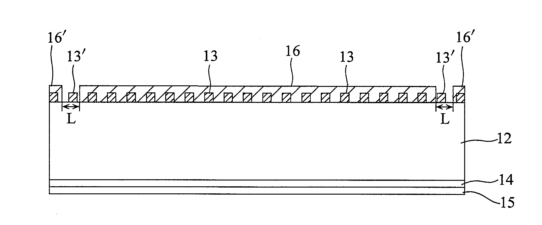
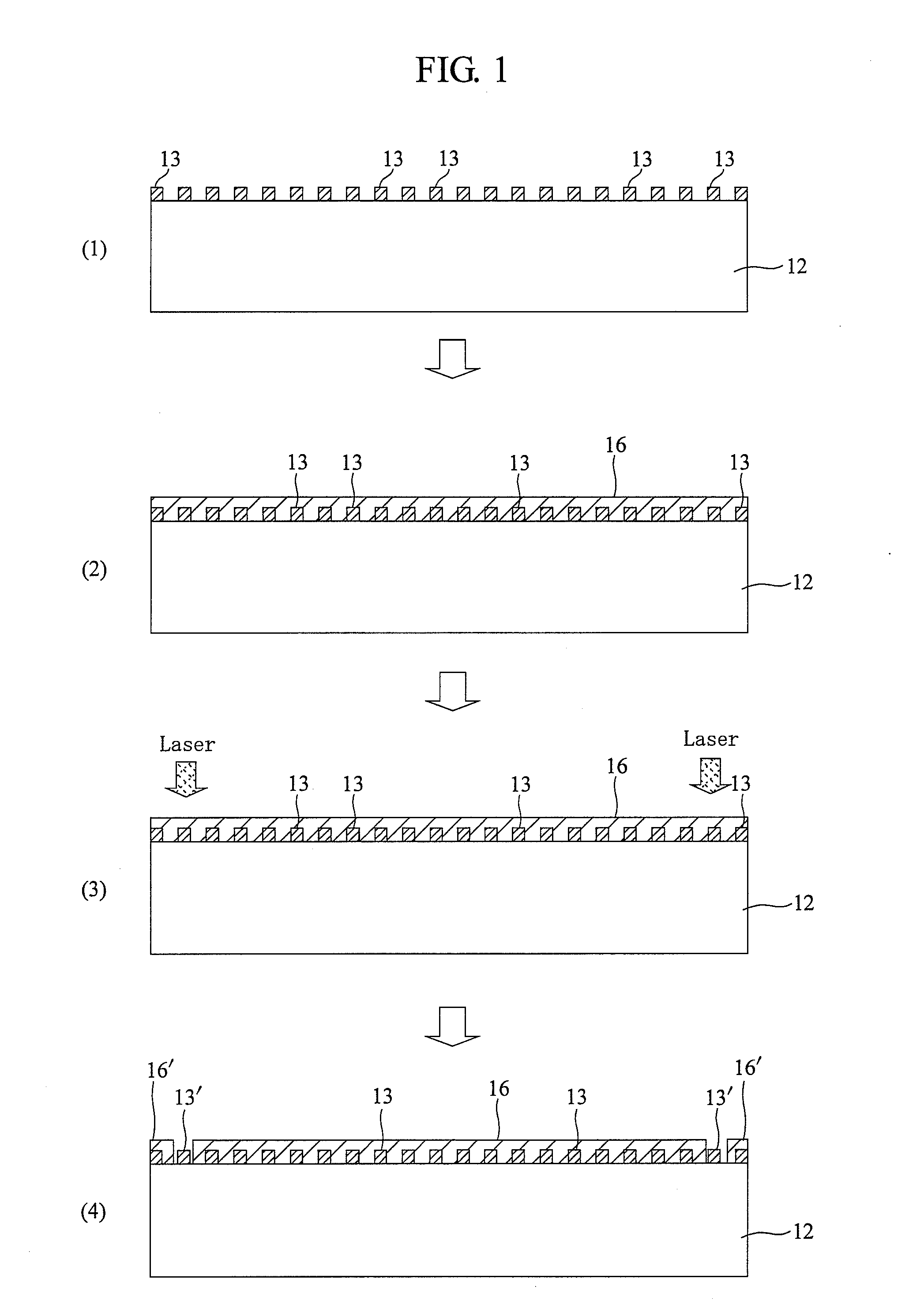
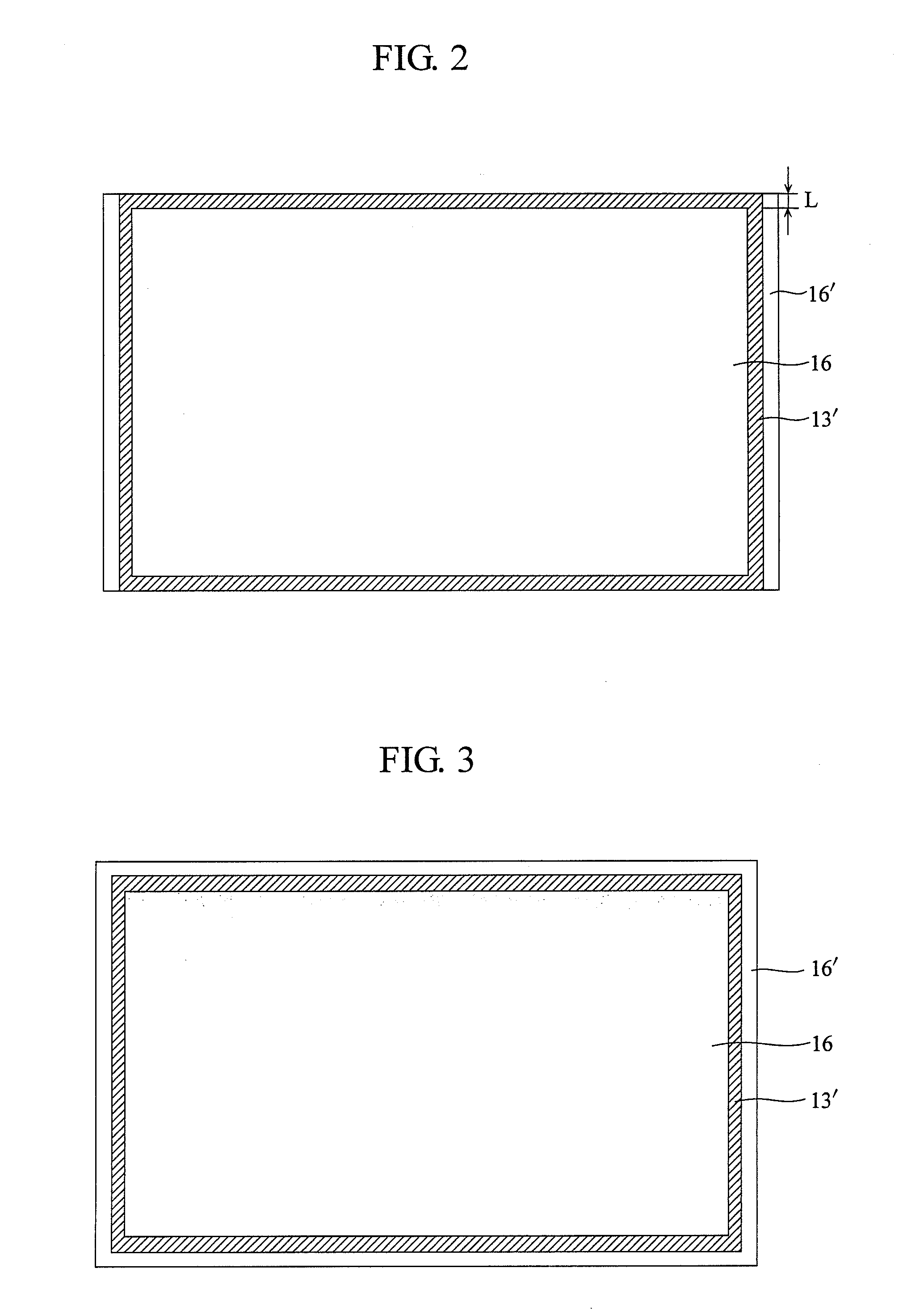
[0203]On an adhesion layer (polyester urethane: thickness of 20 nm) of a continuous polyethylene terephthalate (PET) film having thickness of 100 μm (width of 600 mm, length of 100 m) having the adhesion layer thereon, a polyvinyl alcohol aqueous solution (20%) was printed in dot pattern. A shape of each of the dots was square having a side of 234 μm, a distance between the dots was 20 μm, and the arrangement of the dots was in the form of square grid (lattice). The printed thickness was approx. 5 μm after drying.

[0204]On the PET film having dot pattern, copper was vacuum-deposited to form a copper layer having mean thickness of 4 μm. Subsequently, the PET film having dot pattern and copper layer was immersed in room-temperature water and the dots were dissolved and removed by rubbing with sponge, and then was rinsed with water, dried to form a mesh-shaped conductive metal layer on the whole surface of the PET film (see ...


PUM

PropertyMeasurementUnit
diameteraaaaaaaaaa
wavelengthaaaaaaaaaa

Abstract

[Problem to be Solved]To provide an optical filter for display provided with an earth electrode which can be easily prepared, and a process for the preparation thereof.[Means for Solving Problem]An optical filter for display provided with an electrode part of a conductive metal layer comprising a transparent substrate, the conductive metal layer provided on a surface of the substrate, and a functional layer provided on a surface of the conductive layer, wherein the conductive metal layer is exposed in a large number of island-shaped areas at a side edge or its vicinity of the functional layer, and the number of the island-shaped areas is 25 to 250 / cm2 in an intermittent band-shaped region and an area ratio of the island-shaped areas is 2 to 50% based on the intermittent band-shaped region, the intermittent band-shaped region being defined by a band-shaped area having a perpendicular width between the most inside point and the most outside point of the island-shaped areas, and a process for the preparation thereof.

Description

FIELD OF THE INVENTION[0001]The present invention relates to an optical filter for adding various functions such as antireflection, near-infrared shielding and electromagnetic wave shielding to various displays such as plasma display panel (PDP), cathode-ray-tube (CRT) display, liquid crystal display, organic EL (electroluminescence) display and field emission display (FED) including surface-conduction electron-emitter display (SED), and a display, particularly PDP, provided with the optical filter.DESCRIPTION OF THE RELATED ART[0002]In flat-panel displays such as liquid crystal display, plasma display panel (PDP) and organic EL display, and CRT display, the problem that external light is reflected on a surface of the display to have difficulty seeing visual information of the display has been known. Therefore, various countermeasures including provision of various optical films such as an antireflection film on the displays are taken.[0003]In recent years, image magnification has e...

Claims


Application Information

Patent Timeline
Patent Type & Authority Applications(United States)
IPC IPC(8): G02B1/11B23K26/00H01J17/16H01J17/49
CPCG02B5/223G02B2207/121G02F2201/083H05K9/0096H01J2211/446H01J2329/895H01J11/44
Inventor AOKI, SHIGERU
Owner BRIDGESTONE CORP
Why Eureka
Try Eureka