Laminated Pieozelectric Ceramic Element Manufacturing Method

a technology of piezoelectric ceramics and manufacturing methods, which is applied in the direction of piezoelectric/electrostrictive transducers, transducer types, chemistry apparatus and processes, etc., can solve the problems of difficult to reduce the thickness of a cutting blade for use at the time, high complexity of the manufacturing method described in patent document 1, and the difficulty of reducing the thickness of the cutting blade, etc., to achieve the effect of simplifying the lamination step and the cutting step

Active Publication Date: 2011-02-03
MURATA MFG CO LTD
View PDF0 Cites 8 Cited by
  • Summary
  • Abstract
  • Description
  • Claims
  • Application Information

AI Technical Summary

Benefits of technology

[0020]According to the laminated piezoelectric ceramic element manufacturing method according to the present invention, the first laminated body is cut so as to obtain a plurality of second laminated bodies having the above width-direction dimension, the plurality of second laminated bodies are further laminated to obtain the third laminated body, and the third laminated body is cut in the laminating direction and parallel to the width-direction dimension, to obtain the laminated piezoelectric body, whereby it is possible to simplify the lamination step and the cutting step.
[0021]In the manufacturing method described in Patent Document 1, a plurality of small chips need to be laminated in the laminating direction, thus making the lamination step complicated, and particularly making positioning at the time of lamination complicated. As opposed to this, it is possible to omit the complicated operation of laminating the plurality of chips according to the present invention in consideration of mutual positional relations of the internal electrodes.
[0022]Furthermore, the third laminated body may be cut in the direction parallel to the width direction in the cutting step after lamination of all the internal electrodes, namely the cutting length is the same as the width-direction dimension, whereby it is possible to make the cutting length small as compared with the case of the manufacturing method described in Patent Document 1. This allows enhancement of the cutting precision. Furthermore, it is possible to make the cutting length small and to use a cutting blade having a small thickness. It is thereby possible to reduce materials that are removed due to the cutting, so as to enhance the mass-productivity of the laminated piezoelectric ceramic element.
[0023]FIG. 1 is a perspective view for describing a step of obtaining a first laminated body in a manufacturing method according to an embodiment of the present invention.
[0024]FIG. 2(a) is a perspective view of the first laminated body obtained in the embodiment of the present invention, and FIG. 2(b) is a schematically exploded perspective view for describing a laminated state of internal electrodes in a second laminated body.
[0025]FIG. 3 is a perspective view showing the second laminated body obtained in the embodiment of the present invention.

Problems solved by technology

However, the manufacturing method described in Patent Document 1 is highly complicated.
Moreover, at the time of laminating the plurality of chips 107, the positioning thereof has been highly complicated since the chips 107 are small in size.
Further, due to the necessity to cut the first crimped body 106 having a considerably large thickness, it has been difficult to reduce the thickness of a cutting blade for use at the time of cutting.
It has thus been difficult to increase the number of chips 107 obtained from the first crimped body 106.

Method used


Image

  • Laminated Pieozelectric Ceramic Element Manufacturing Method
  • Laminated Pieozelectric Ceramic Element Manufacturing Method
  • Laminated Pieozelectric Ceramic Element Manufacturing Method

Examples


Embodiment Construction

[0053]Hereinafter, specific embodiments of the present invention are described, with reference to the drawings, to demonstrate the present invention.

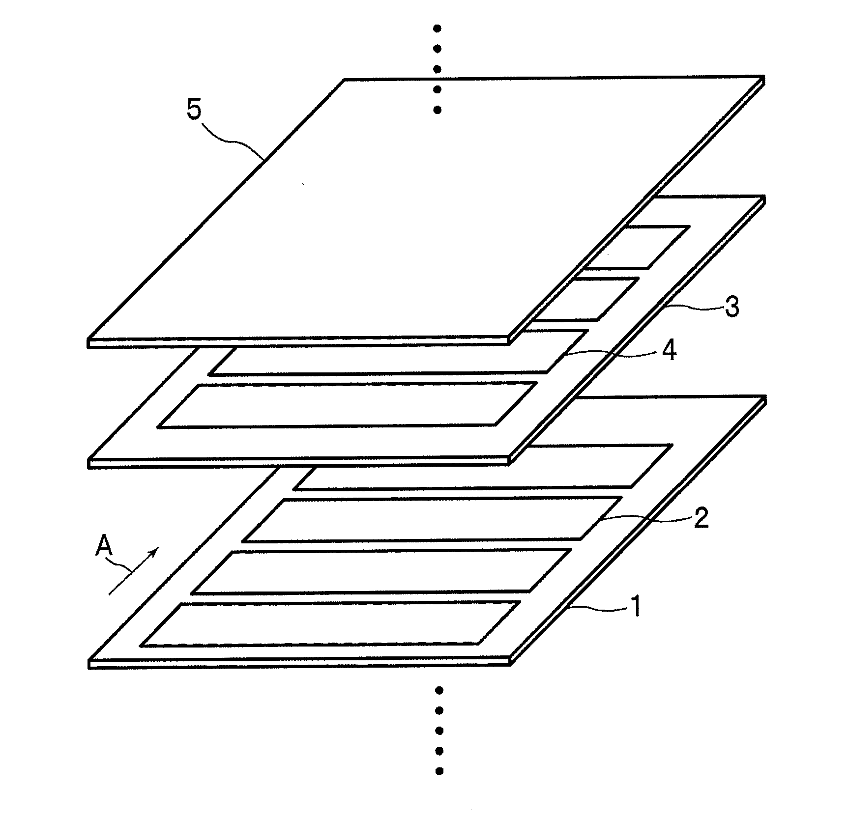
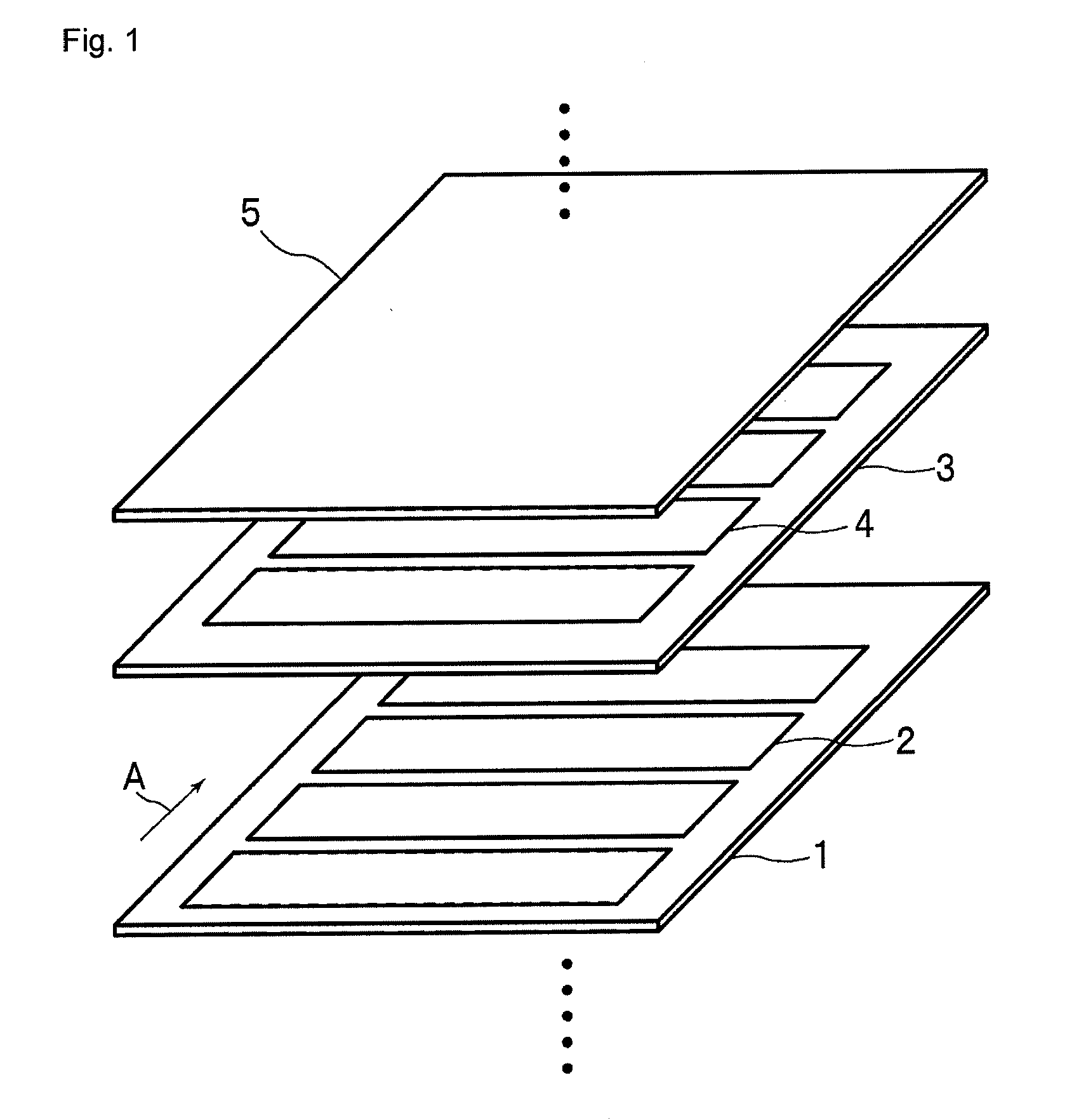
[0054]A laminated piezoelectric ceramic element manufacturing method according to an embodiment of the present invention will be described with reference to FIGS. 1 to 8.

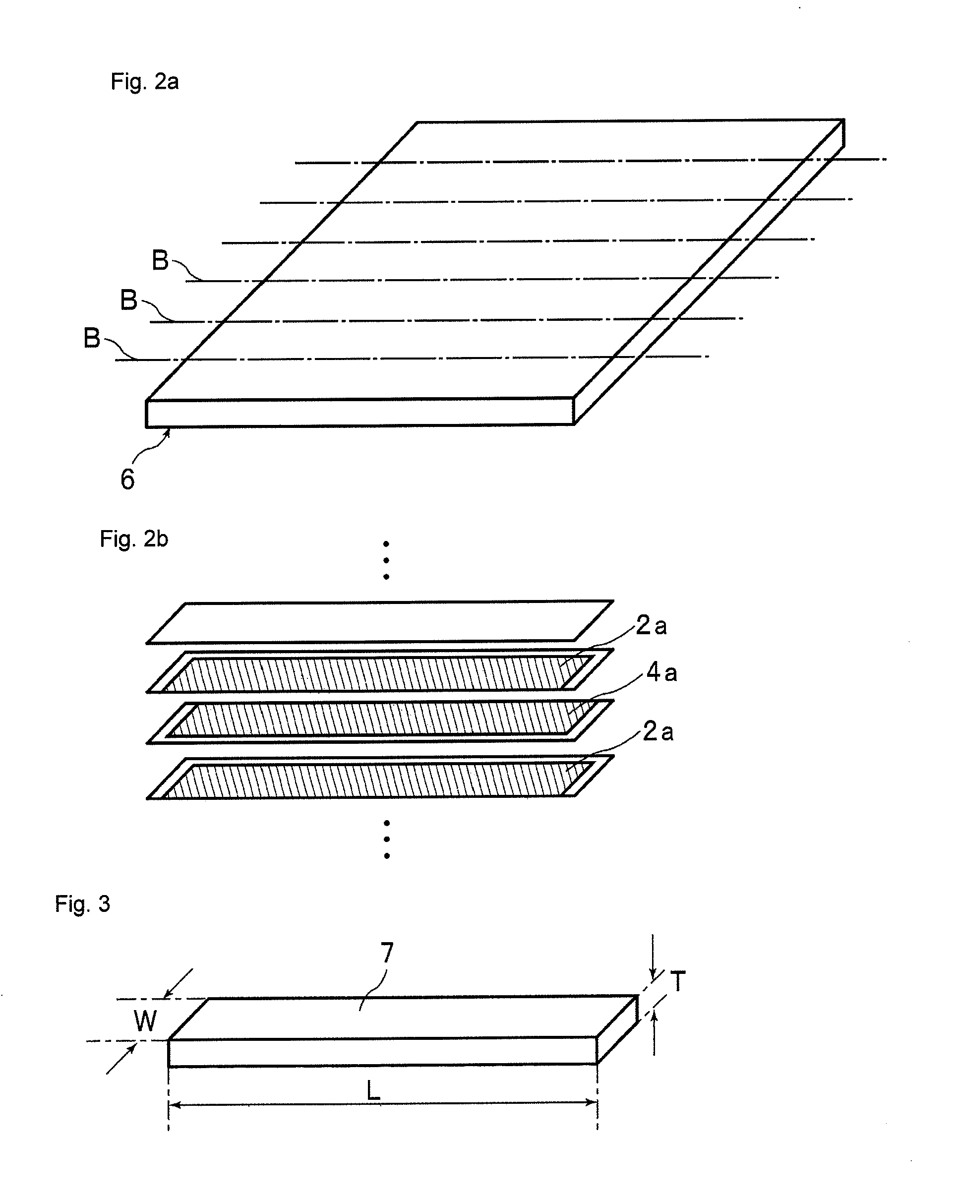
[0055]In the present embodiment, first, a ceramic slurry containing a lead zirconate titanate (PZT) powder as a piezoelectric ceramic powder, a resin binder, and a dispersant is molded into a sheet, to obtain a ceramic green sheet. On this ceramic green sheet, an internal electrode pattern is printed which includes a plurality of internal electrodes each in a stripe-like shape, namely, a longitudinal rectangle. At the time of printing the internal electrode pattern, there is used a method for printing a conductive paste containing a metal powder such as an Ag—Pd powder on the above ceramic green sheet by screen printing or the like. However, printing of internal electro...


PUM

PropertyMeasurementUnit
thicknessaaaaaaaaaa
temperatureaaaaaaaaaa
pressureaaaaaaaaaa

Abstract

There is provided a laminated piezoelectric ceramic element manufacturing method, wherein, even when the number of internal electrode laminations is increased, the lamination and cutting steps can be simplified, to enhance cutting precision and make cutting cost low. A first laminated body having stripe-like internal electrodes is cut into a plurality of second laminated bodies so as to have a width-direction dimension W corresponding to a width dimension of a laminated piezoelectric ceramic element chip to be ultimately obtained. Two or more second laminated bodies are laminated in the laminating direction to obtain a third laminated body, and the third laminated body is cut in the laminating direction and parallel to the width direction W to obtain a laminated piezoelectric body.

Description

[0001]This is a continuation of application Serial No. PCT / jp2009 / 000952, filed Mar. 3, 2009, the contents of which are incorporated herein by reference.TECHNICAL FIELD[0002]The present invention relates to a laminated piezoelectric ceramic element manufacturing method used for a laminated piezoelectric resonator, a laminated piezoelectric filter and the like, and more specifically, the present invention relates to a laminated piezoelectric ceramic element manufacturing method including a step of cutting a mother laminated body and a step of obtaining individual laminated piezoelectric bodies for laminated piezoelectric ceramic elements.BACKGROUND ART[0003]There has previously been used a laminated piezoelectric actuator for driving a head of a hard disc drive, a head of a printer, and the like.[0004]The number of internal electrodes in the laminated piezoelectric actuators have been on the increase, to obtain a larger amount of displacement. Further, a piezoelectric body layer betw...

Claims


Application Information

Patent Timeline
Patent Type & Authority Applications(United States)
IPC IPC(8): H01L41/22H01L41/273H01L41/338H01L41/39
CPCH01L41/083H03H3/02H03H9/178Y10T156/13H01L41/338Y10T29/42Y10T156/1075H01L41/273H10N30/50H10N30/053H10N30/088
Inventor ASANO, HIROSHIHORIKAWA, KATSUHIROTAKATA, MASACHIKAKATO, MASANORI
Owner MURATA MFG CO LTD
Why Eureka
Try Eureka