Bulk heterojunction solar cell and method of manufacturing the same

a solar cell and heterojunction technology, applied in the field of bulk heterojunction solar cells, can solve the problems of low efficiency, poisonous cd itself, large difference between lattice constants and energy band gaps between two materials, etc., and achieve the effect of reducing manufacturing costs and greatly increasing the power output of solar cells

Inactive Publication Date: 2011-02-03
RES COOPERATION FOUND OF YEUNGNAM UNIV
View PDF4 Cites 32 Cited by
  • Summary
  • Abstract
  • Description
  • Claims
  • Application Information

AI Technical Summary

Benefits of technology

[0037]As described above, in the bulk heterojunction solar cell and the method of manufacturing the same according to the present invention, firstly, instead of forming a p-type semiconductor and an n-type semiconductor as a thin layer, a porous p-type semiconductor layer is formed by sintering CIGS powders, and then, the n-type semiconductor is coated on the surface of the CIGS powders by using a wet method such that a much larger junction area than a physical size of the solar cell is formed and a power output of the solar cell can be greatly increased. Secondly, when Al:ZnO as a conductive transparent electrode is formed by sputtering as a general method, Al:ZnO cannot be uniformly coated on the inside of the p-type semiconductor. However, according to the present invention, Al:ZnO is grown by using CBD such that ZnO / CdS can be uniformly coated on the entire surface of the CIGS powders by using the wet method. Thirdly, the solar cell can be manufactured under room pressure such that manufacturing costs can be remarkably reduced.

Problems solved by technology

However, two materials have a large difference in both lattice constants and energy band gaps.
The drawback of CdS is that Cd itself is poisonous and a wet chemical process is used to form the CdS thin film unlike in other unit thin films.
CuInSe2 that is a three-component compound and has been used for the light absorption layer 30 in the early of development, has an energy band gap of 1.04 eV and has a high short circuit current but has a low open voltage, which results in low efficiency.
In this way, the CIGS thin film is a multicomponent compound and thus, a process of manufacturing the same is very complicated.
Solar rays are not absorbed into the area of the grid electrode 70, which results in a loss of efficiency.
Furthermore, the photoelectric conversion efficiency of the thin film solar cells having a restricted area is limited.
Therefore, higher photoelectric conversion efficiency compared to the pn-junction side cannot be obtained.

Method used


Image

  • Bulk heterojunction solar cell and method of manufacturing the same
  • Bulk heterojunction solar cell and method of manufacturing the same
  • Bulk heterojunction solar cell and method of manufacturing the same

Examples


Embodiment Construction

[0045]The present invention will now be described more fully with reference to the accompanying drawings, in which exemplary embodiments of the invention are shown. First, terms or words used in the present specification and the claims should not be construed as being limited to general or literal meaning, and the inventor should construe his / her own invention in meaning and concept that coincide with the technical spirit of the invention based on the principle for properly defining the concept of the terms so as to describe his / her own invention in the best manner.

[0046]Thus, configurations shown in embodiments and the drawings of the present invention rather are an example of the most exemplary embodiment and does not represent all of the technical spirit of the invention. Thus, it will be understood that various equivalents and modifications that replace the configurations are possible when filing the present application.

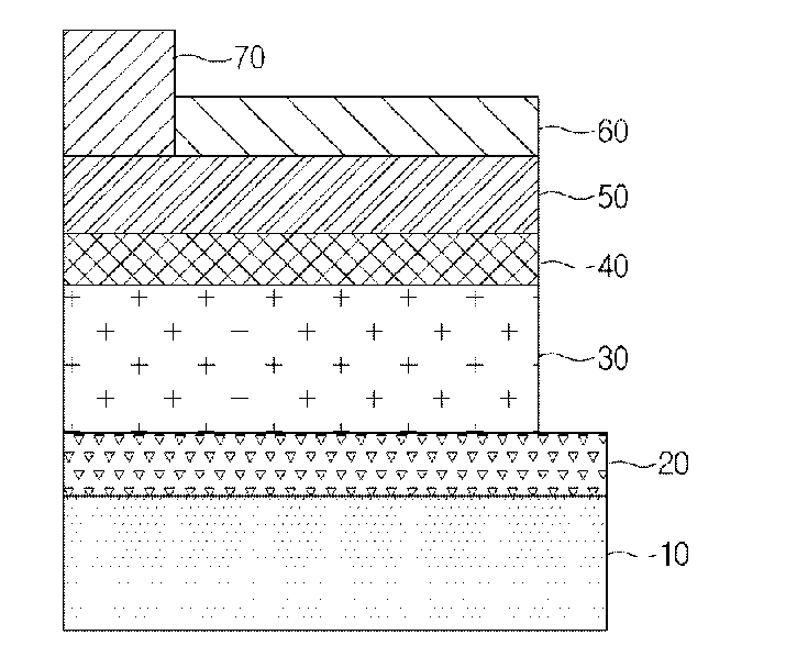
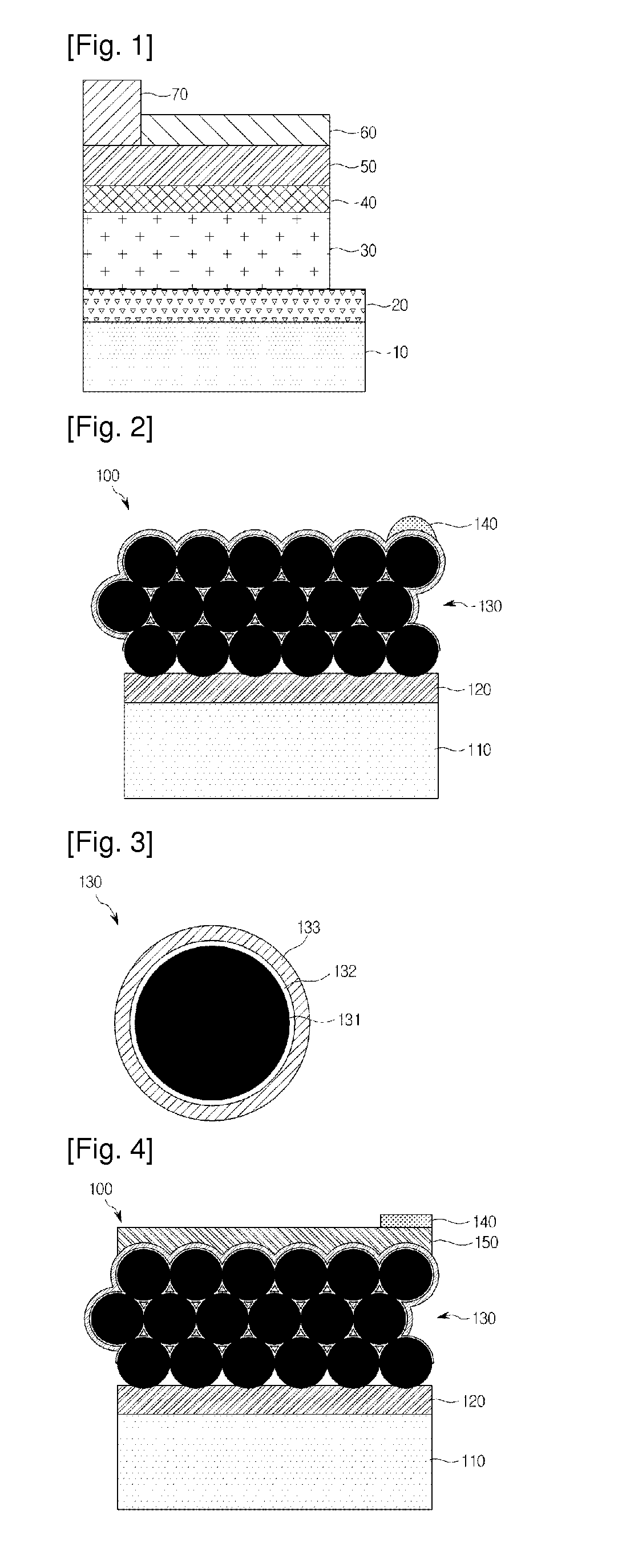
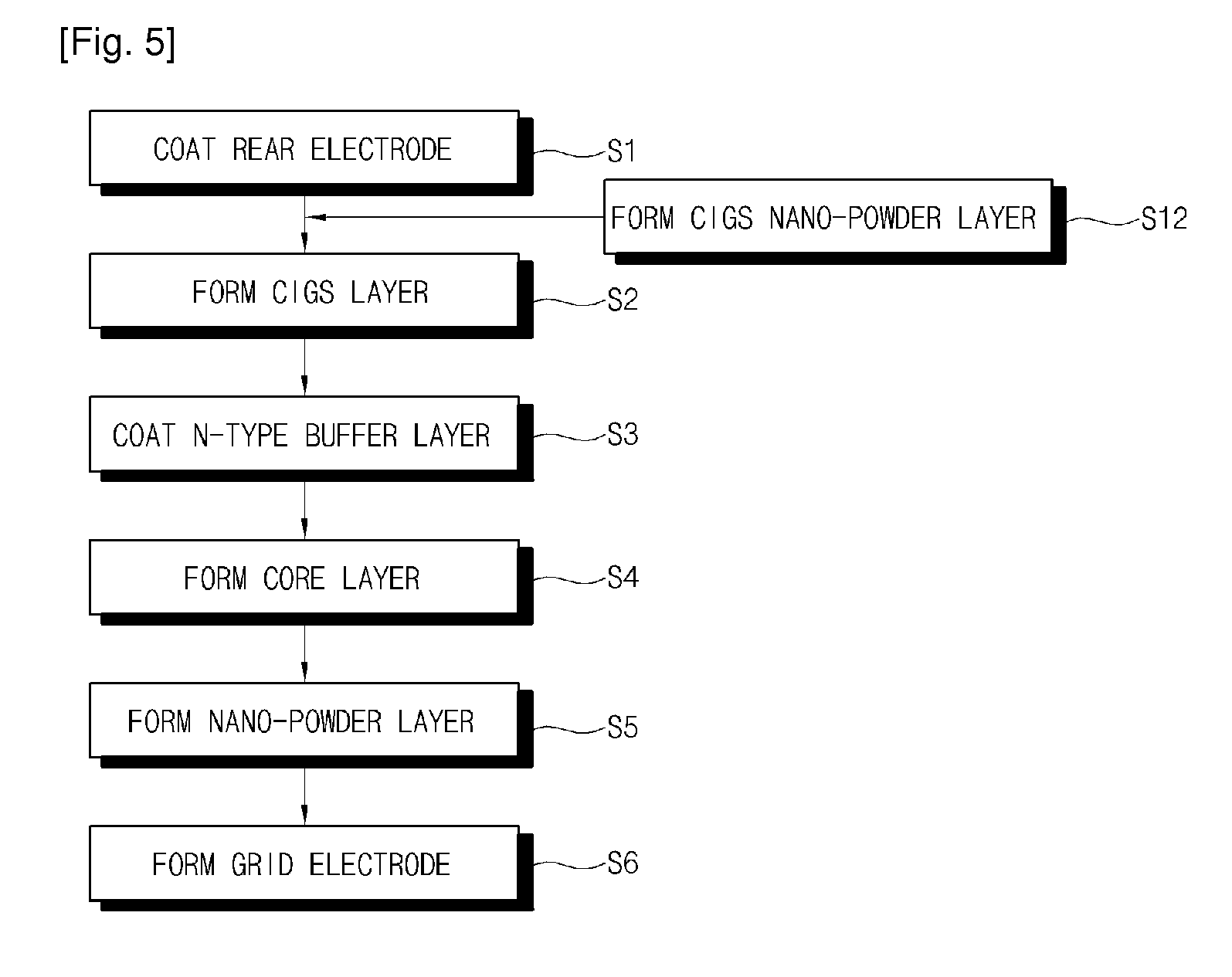
[0047]Hereinafter, a bulk heterojunction solar cell 100 acc...


PUM

PropertyMeasurementUnit
thicknessaaaaaaaaaa
thicknessaaaaaaaaaa
thicknessaaaaaaaaaa

Abstract

Provided are a bulk heterojunction solar cell, including: a substrate; a rear electrode formed on a top surface of the substrate; a core layer comprising a copper indium gallium diselenide (CIGS) layer in which a CIGS powder is formed on a top surface of the rear electrode to be porous, an n-type buffer layer coated on the CIGS powder, and an n-type ZnO layer coated on the n-type buffer layer; and a grid electrode formed on a top surface of the core layer, and a method of manufacturing the same. A porous p-type semiconductor layer is formed by sintering CIGS powders, and then, the n-type semiconductor is coated on the surface of the CIGS powders by using a wet method such that a much larger junction area than a physical size of the solar cell is formed and a power output of the solar cell can be greatly increased.

Description

TECHNICAL FIELD[0001]The present invention relates to a bulk heterojunction solar cell and a method of manufacturing the same, and more particularly, to a bulk heterojunction solar cell in which a larger junction area than the area of a substrate is formed to maximize photoelectric conversion efficiency, and a method of manufacturing the same.BACKGROUND ART[0002]I-III-VI2 group chalcopyrite-based compound semiconductors that are generally represented as CuInSe2 have a direct transition type energy band gap and have the highest light absorption coefficient of 1×105 cm−1. Thus, in the I-III-VI2 group chalcopyrite-based compound semiconductors, high-efficiency solar cells can be manufactured with a thin film having a thickness of 1 to 2 μm, and long-term electro-optic stability is very excellent.[0003]For this reason, the chalcopyrite-based compound semiconductors are being focused on as a material used in forming low-cost and high-efficiency solar cells that remarkably improve economi...

Claims


Application Information

Patent Timeline
Patent Type & Authority Applications(United States)
IPC IPC(8): H01L31/0264H01L31/0749
CPCH01L31/022425Y02E10/541H01L31/0749Y02P70/50H01L31/0216H01L31/04
Inventor JEON, CHAN WOOK
Owner RES COOPERATION FOUND OF YEUNGNAM UNIV
Why Eureka
Try Eureka