High-Frequency Module and Method of Manufacturing the Same, and Transmitter, Receiver, Transceiver, and Radar Apparatus Comprising the High-Frequency Module

a high-frequency module and manufacturing method technology, applied in pulse techniques, instruments, waveguides, etc., can solve problems such as instability in positioning accuracy, occurrence of significant positional deviation, and poor visibility of input-output ports, and achieve the effect of reducing loss

Inactive Publication Date: 2011-02-03
KYOCERA CORP
View PDF8 Cites 14 Cited by
  • Summary
  • Abstract
  • Description
  • Claims
  • Application Information

AI Technical Summary

Benefits of technology

[0009]An object of the invention is to provide a high-frequency module capable of making high-frequency connection between a circuit board and a substrate having an input-output portion configured to input and output high-frequency signals stably with lower loss and a method of manufacturing a high-frequency module, as well as to provide a transmitter, a receiver, a transceiver, and a radar apparatus comprising the high-frequency module.

Problems solved by technology

Therefore, at the time of positioning of the input-output port and the waveguide or positioning of mutually-corresponding input-output ports, the input-output port is poorly visible.
This leads to instability in positioning accuracy with consequent possibility of occurrence of significant positional deviation.
In the local area of the transmission path subjected to variation, reflection of a high-frequency signal or the like occurs, which may give rise to a problem of an increase in transmission loss.
Furthermore, the larger is the number of the input-output ports, the larger is the number of solder bumps which are used for connection of the input-output ports, with consequent complication of mounting process steps.

Method used


Image

  • High-Frequency Module and Method of Manufacturing the Same, and Transmitter, Receiver, Transceiver, and Radar Apparatus Comprising the High-Frequency Module
  • High-Frequency Module and Method of Manufacturing the Same, and Transmitter, Receiver, Transceiver, and Radar Apparatus Comprising the High-Frequency Module
  • High-Frequency Module and Method of Manufacturing the Same, and Transmitter, Receiver, Transceiver, and Radar Apparatus Comprising the High-Frequency Module

Examples


first embodiment

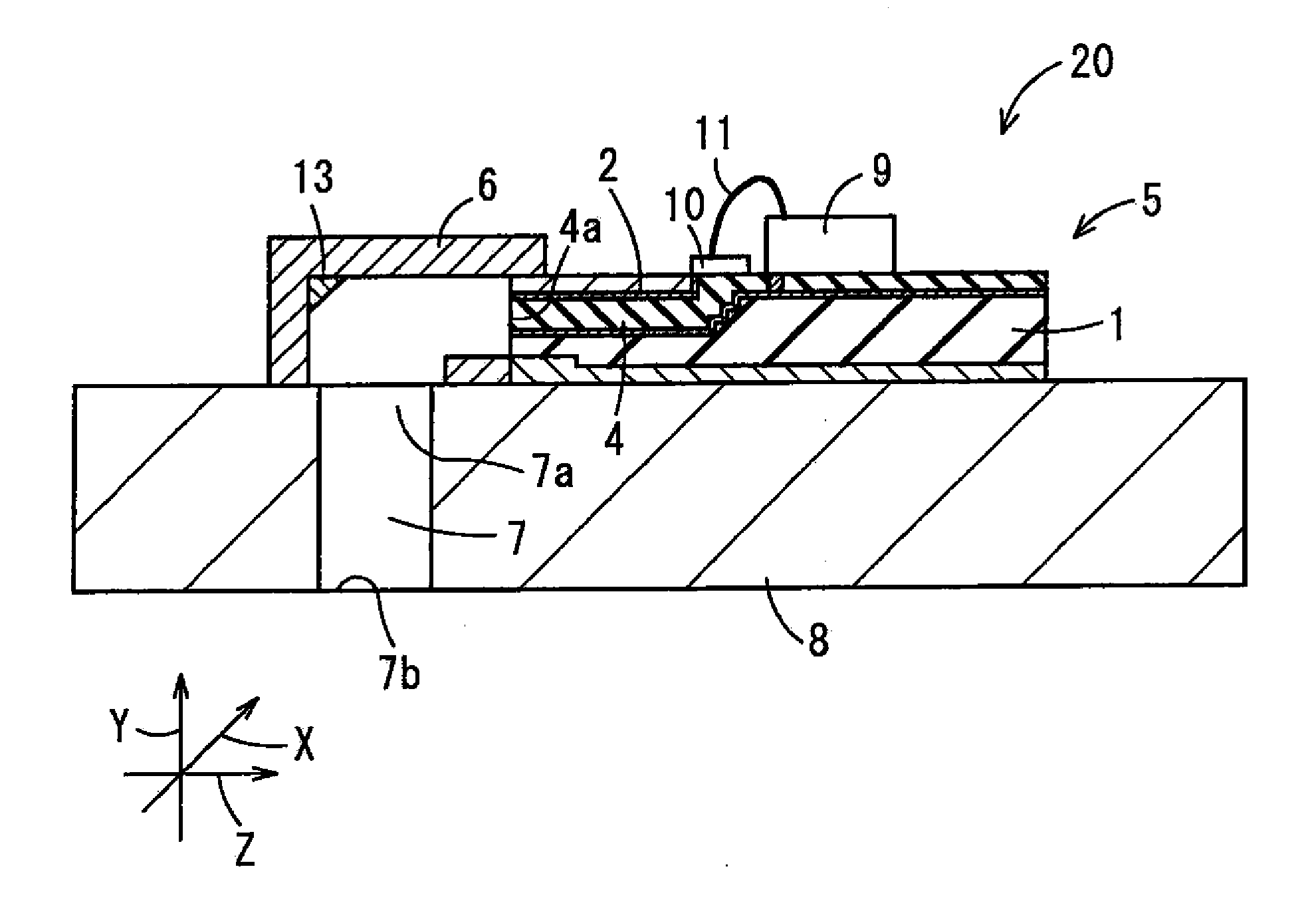
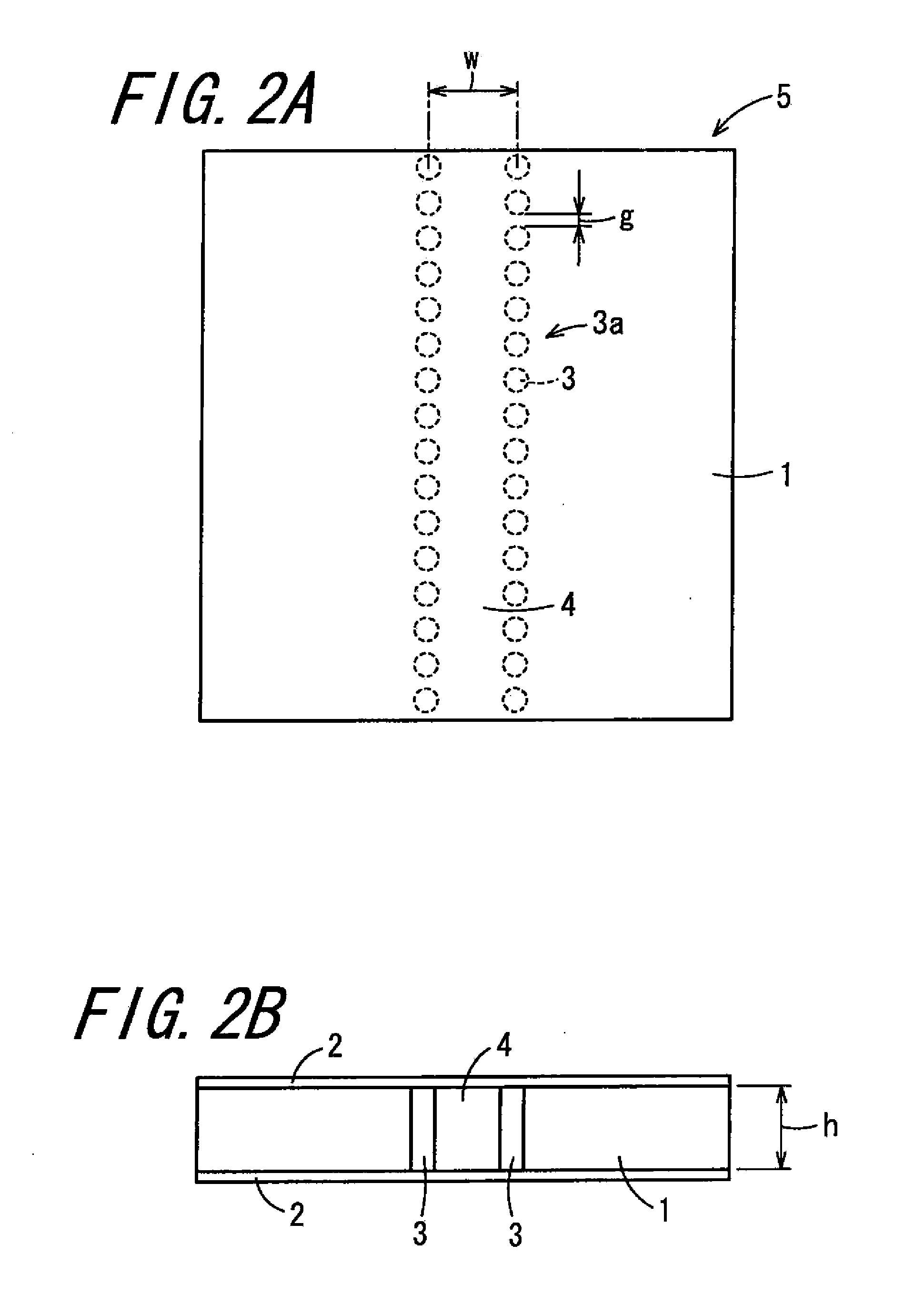
[0063]FIG. 1 is a diagram showing the structure of a high-frequency module 20 in accordance with the invention. Moreover, FIGS. 2A and 2B are diagrams showing the structure of a circuit board 5. FIG. 2A is a top view of the circuit board 5, and FIG. 2B is a side view of the circuit board 5 as viewed in a direction of high-frequency signal transmission. The high-frequency module 20 includes the circuit board 5, a waveguide 6, and a substrate 8 having a first input-output portion (a first input-output port 7a) for high-frequency signals formed on one surface thereof.

[0064]The circuit board 5 comprises a dielectric, layer 1, a pair of conductor layers 2 opposed to each other, with the dielectric layer 1 lying therebetween, and a through conductor group 3a that electrically connects the pair of conductor layers 2. The through conductor group 3a comprises a plurality of through conductors 3 passing all the way through the dielectric layer 1 to establish electrical connection between the ...

second embodiment

[0085]FIG. 3 is a diagram showing the structure of a high-frequency module 21 in accordance with the invention. The high-frequency module 21 is analogous to the above-described high-frequency module 20, and thus like components will be identified with the same reference symbols and overlapping descriptions will be omitted. In the high-frequency module 21, the waveguide 6 is provided with pin-shaped adjustment elements 12 which are displaceable in each of the X-axis direction, the Y-axis direction, and the Z-axis direction within the cavity of the waveguide 6. By causing displacement of the adjustment elements 12 along a longitudinal direction thereof, the frequency of a high-frequency signal to be transmitted through the waveguide 6 can be adjusted. Note that the adjustment element 12 may be placed along at least one of the X-axis direction, the Y-axis direction, and the Z-axis direction.

[0086]Next, a method of manufacturing the high-frequency module 20, 21 will be described. To beg...

third embodiment

[0093]FIG. 4 is a sectional view showing the structure of a high-frequency module 100 in accordance with the invention. FIG. 5 is a front view showing the structure of the high-frequency module 100. In this embodiment, the same components as those in the preceding embodiment will be identified with the same reference symbols, and the description thereof will be omitted. The high-frequency module 100 includes a circuit board 120, the substrate 8 (antenna board) having the first input-output port 7a formed on one surface thereof, and a sealing structure 108 serving as a waveguide.

[0094]The circuit board 120 is a board in which a planar line 10 and a stacked waveguide line 102, which is a dielectric waveguide line formed within the dielectric layer 1, are electrically connected to each other thereby forming a high-frequency circuit. The planar line 10 is one of lines for transmission of high-frequency signals in a microwave band or a millimeter-wave band, and is more specifically desig...


PUM

PropertyMeasurementUnit
frequencyaaaaaaaaaa
frequencyaaaaaaaaaa
temperaturesaaaaaaaaaa

Abstract

A high-frequency module according to the present embodiment includes a substrate, a circuit board, and a waveguide. The substrate has an input-output portion for high-frequency signals on one surface thereof. The circuit board has a dielectric waveguide line with its end face exposed, and is placed on the one surface of the substrate such that a virtual plane extending beyond the end face is intersected by the one surface of the substrate. The waveguide has openings at ends thereof, in which one of the openings is connected to the end face of the dielectric waveguide line, and the other opening is connected to the input-output portion of the substrate.

Description

TECHNICAL FIELD[0001]The present invention relates to a high-frequency module for use in communication equipment and a method of manufacturing the high-frequency module, and also a transmitter, a receiver, a transceiver, and a radar apparatus comprising the high-frequency module.BACKGROUND ART[0002]In order to achieve high-speed transmission of large-volume data, there have been proposed systems based on information-communication equipment that utilizes a high-frequency range such as a microwave range of 1 to 30 GHz and a millimeter-wave range of 30 to 300 GHz. In addition, millimeter wave-using systems and the like such as a radar apparatus that measures inter-vehicle distance have been proposed to date.[0003]As a high-frequency circuit board structure adopted in such equipment utilizing a high-frequency range such as a microwave range and a millimeter-wave range, a monolithic microwave integrated circuit (MMIC) and a structure in which a passive electronic component is mounted on ...

Claims


Application Information

Patent Timeline
Patent Type & Authority Applications(United States)
IPC IPC(8): G01S13/58H01P3/16H05K3/00H04L27/00H04B1/38G01S7/03G01S7/35G01S13/02H01P1/02H01P1/04H01P3/12H01P5/107
CPCG01S7/032Y10T29/49128H01P5/107H01P3/121
Inventor SAGALA, DJUNIADI A.HAYATA, KAZUKIKISHIDA, YUJI
Owner KYOCERA CORP
Why Eureka
Try Eureka