Method for fabricating copper-containing ternary and quaternary chalcogenide thin films

a technology of ternary and quaternary chalcogenide and thin film, which is applied in the direction of liquid/solution decomposition chemical coating, coating, semiconductor devices, etc., can solve the problems of limiting electrical performance characteristics, non-stoichiometric proportions, and deposited films often include relatively high defect densities, so as to improve physical, chemical, optical, and easy control

Inactive Publication Date: 2011-02-03
QUANTUMSCAPE CORP
View PDF6 Cites 36 Cited by
  • Summary
  • Abstract
  • Description
  • Claims
  • Application Information

AI Technical Summary

Benefits of technology

[0029]Objects of the invention include the following: providing a bath deposition apparatus capable of depositing a selected phase on a substrate while minimizing homogeneous nucleation of the same or similar phase within the bulk of the fluid bath; providing a bath deposition apparatus capable of depositing films having improved physical, chemical, optical, or electrical properties; providing a bath deposition apparatus that is more easily controlled; providing a bath deposition apparatus that uses reagents more efficiently; providing a bath deposition apparatus that allows localized heating of a relatively small volume of the bath while maintaining the remainder of the bath at a relatively lower temperature; providing a bath deposition apparatus for growing high quality mixed chalcogenide thin films; providing a bath deposition apparatus for growing mixed Cu-containing chalcogenide films suitable for photovoltaic cells; providing a method for bath deposition that is more easily controlled; providing a method for bath deposition that minimizes homogeneous nucleation within the bath; providing a method for bath deposition capable of depositing films of selected II-VI compounds, other compounds, or metals having improved properties; providing a method for bath deposition of high quality mixed Cu-containing chalcogenide films; and, providing a method for bath deposition of chalcogenide films having a graded composition. These and other objects will become apparent on reading the specification in conjunction with the accompanying drawings.
[0030]In accordance with one aspect of the invention, an apparatus for depositing a solid film onto a substrate from reagent solutions comprises:
[0031]a reservoir of a first reagent solution maintained at a first temperature at which homogeneous reactions are substantially inhibited within the first reagent solution;
[0032]a first showerhead assembly including a nebulizer configured to dispense the first reagent solution as a fine mist at the first temperature;
[0033]a reservoir of a second reagent solution maintained at a second temperature at which homogeneous reactions are substantially inhibited within the second reagent solution;
[0034]a second showerhead assembly configured to dispense the second reagent solution as a flowing stream at the second temperature;

Problems solved by technology

), are non-equilibrium, often resulting in non-stoichiometric proportions.
Also, due to the nature of the deposition processes, the deposited films often include relatively high defect densities.
In the case of semiconducting devices, such high defect levels can limit electrical performance characteristics.
In semiconductor device fabrication wherein p-n junctions are formed in a partial vacuum by depositing one film over a second film or a substrate of different conductivity type, the conventional evaporative and sputtering techniques may provide unsatisfactory film qualities.
As an alternative, relatively more expensive techniques such as Chemical Vapor Deposition (CVD), Molecular Beam Epitaxy (MBE), pulsed laser deposition, and atomic layer epitaxy, are useful, especially with formation of III-V compound semiconductor materials, but satisfactory deposition processes have not been available for fabrication of thin film II-VI compound semiconductor materials.
Bringing devices based on these materials to the market has been greatly impacted by the cumbersome and poor yield of their traditional growth techniques.
All the above are expensive vacuum techniques; and the process involved is based mostly on the intermixing of elements constituting the material and subjecting the mixture to high temperature to form the compound.
Unfortunately each of the various elemental particles does not have the same surrounding.
Hence, small isolated areas will have the right material composition after anneal leading to film with non-uniform stoichiometry.
Thus, the process may be good for small area deposition but poor for large area deposition needed for high yield manufacturing.
Both of the foregoing methods are non-trivial, as they involve nanoparticle growth, a process which is not as cheap as one expects, because the nanoparticle growth requires expensive chemicals and takes place at extremely slow rate.
This is then followed by the expensive ink formulation process.
Materials grown by this method will also suffer from non uniformity due to high probability of particles not having the correct surrounding particles throughout the growth area.
However, the single precursor is a very expensive organometallic (PPh3)2Cu(SEt)2In(SEt)2.
The high precursor cost may not be compatible with the low cost devices like solar cells [5].
This slow growth rate and the accompanying waste make this process unacceptable [6].

Method used


Image

  • Method for fabricating copper-containing ternary and quaternary chalcogenide thin films
  • Method for fabricating copper-containing ternary and quaternary chalcogenide thin films
  • Method for fabricating copper-containing ternary and quaternary chalcogenide thin films

Examples


example

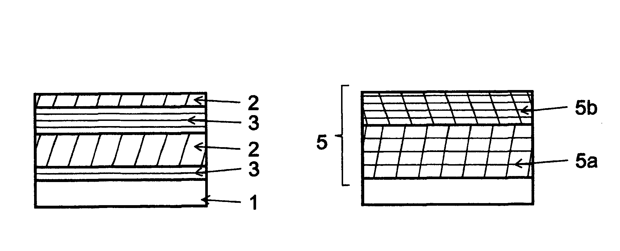
[0084]A graded film consisting predominantly of the phase Cu2ZnSnS4 was deposited on Mo-coated stainless steel in the sequence CuS—SnZnS—CuS—SnZnS. For VPSPEED SnZnS deposition, the reagent solution consists of SnCl3 0.0025M, zinc nitrate 0.0025M, and thiourea 0.0075M in 1:1 ethanol-de-ionized water solution maintained at 15° C.; tions, and the substrate kept at 160° C. For LPSPEED CuS deposition, the aqueous reagent solution consisting of copper sulfate 0.005M, triethanolamine 0.09M, citric acid 0.125M, nitriotriacetic acid 0.03M and thioacetamide 0.008M was used. This reagent solution was maintained at 15° C. and dispensed onto the heated substrate, which was held at about 120° C. The complete grown film was then annealed in Ar / N2 ambient at about 210° C. for about 10 minutes.

[0085]The resulting film, about 0.8 μm thick, was analyzed by SIMS and the depth profile is shown in FIG. 7. It can be seen that Cu and S are fairly uniformly distributed throughout the film, whereas Sn and Z...


PUM

PropertyMeasurementUnit
temperaturesaaaaaaaaaa
droplet sizeaaaaaaaaaa
temperatureaaaaaaaaaa

Abstract

An apparatus for depositing a solid film onto a substrate from a reagent solution includes reservoirs of reagent solutions maintained at a sufficiently low temperature to inhibit homogeneous reactions within the reagent solutions. The chilled solutions are dispensed through showerheads, one at a time, onto a substrate. One of the showerheads includes a nebulizer so that the reagent solution is delivered as a fine mist, whereas the other showerhead delivers reagent as a flowing stream. A heater disposed beneath the substrate maintains the substrate at an elevated temperature at which the deposition of a desired solid phase from the reagent solutions may be initiated. Each reagent solution contains at least one metal and either S or Se, or both. At least one of the reagent solutions contains Cu. The apparatus and its associated method of use are particularly suited to forming films of Cu-containing compound semiconductors.

Description

BACKGROUND OF THE INVENTION[0001]1. Field of the Invention[0002]The invention pertains to a system and method for chemically coating a variety of surfaces with semiconductor materials, metals, or insulators for various applications including electronics. More particularly, the invention pertains to methods for making chalcogenide compound films containing copper, for photovoltaic devices and other applications.[0003]2. Description of Related Art[0004]Numerous coating processes like electroless chemical, chemical vapor, and physical vapor depositions are commonly employed in industrial applications. Physical vapor deposition is commonly used in semiconductor manufacturing applications, often employing expensive vacuum techniques in order to sustain a relatively high film growth rate. Many such processes, while performed at high temperatures (e.g., greater than 300° C.), are non-equilibrium, often resulting in non-stoichiometric proportions. Also, due to the nature of the deposition p...

Claims


Application Information

Patent Timeline
Patent Type & Authority Applications(United States)
IPC IPC(8): H01L21/36H01L21/20B05C11/00
CPCC23C18/1204C23C18/1258C23C18/1283H01L21/67207C23C18/1295H01L21/02568H01L21/02628C23C18/1291H01L21/00H01L21/02C23C18/12
Inventor OLADEJI, ISAIAH O.
Owner QUANTUMSCAPE CORP
Why Eureka
Try Eureka