Manufacturing method of semiconductor device including etching step

a manufacturing method and semiconductor technology, applied in the direction of manufacturing tools, coatings, instruments, etc., can solve the problems of difficult to improve the etching speed and the etching rate, and achieve the effect of reducing manufacturing time and improving etching speed

Inactive Publication Date: 2011-02-10
DENSO CORP
View PDF5 Cites 25 Cited by
  • Summary
  • Abstract
  • Description
  • Claims
  • Application Information

AI Technical Summary

Benefits of technology

[0008]In the above case, the poly crystallized portion has a penetration speed and an adsorption speed of the etchant, which are higher th

Problems solved by technology

However, since an etching rate of the intermediate layer made of oxide silicon is low, and the upper

Method used


Image

  • Manufacturing method of semiconductor device including etching step
  • Manufacturing method of semiconductor device including etching step
  • Manufacturing method of semiconductor device including etching step

Examples


Embodiment Construction

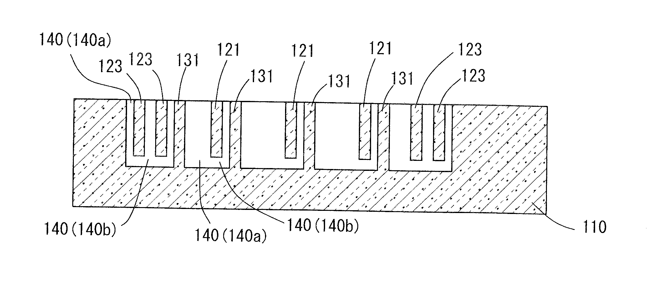
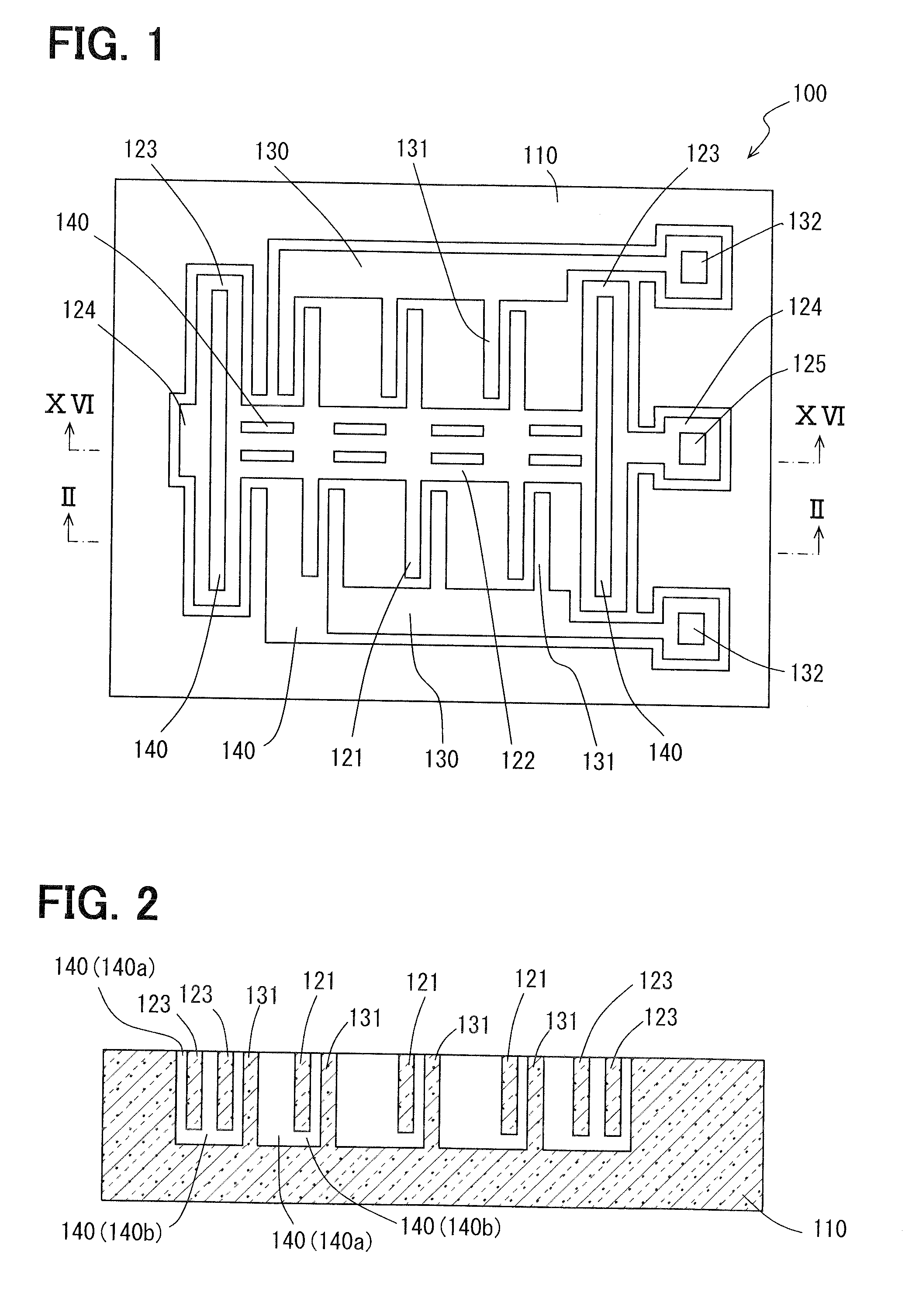
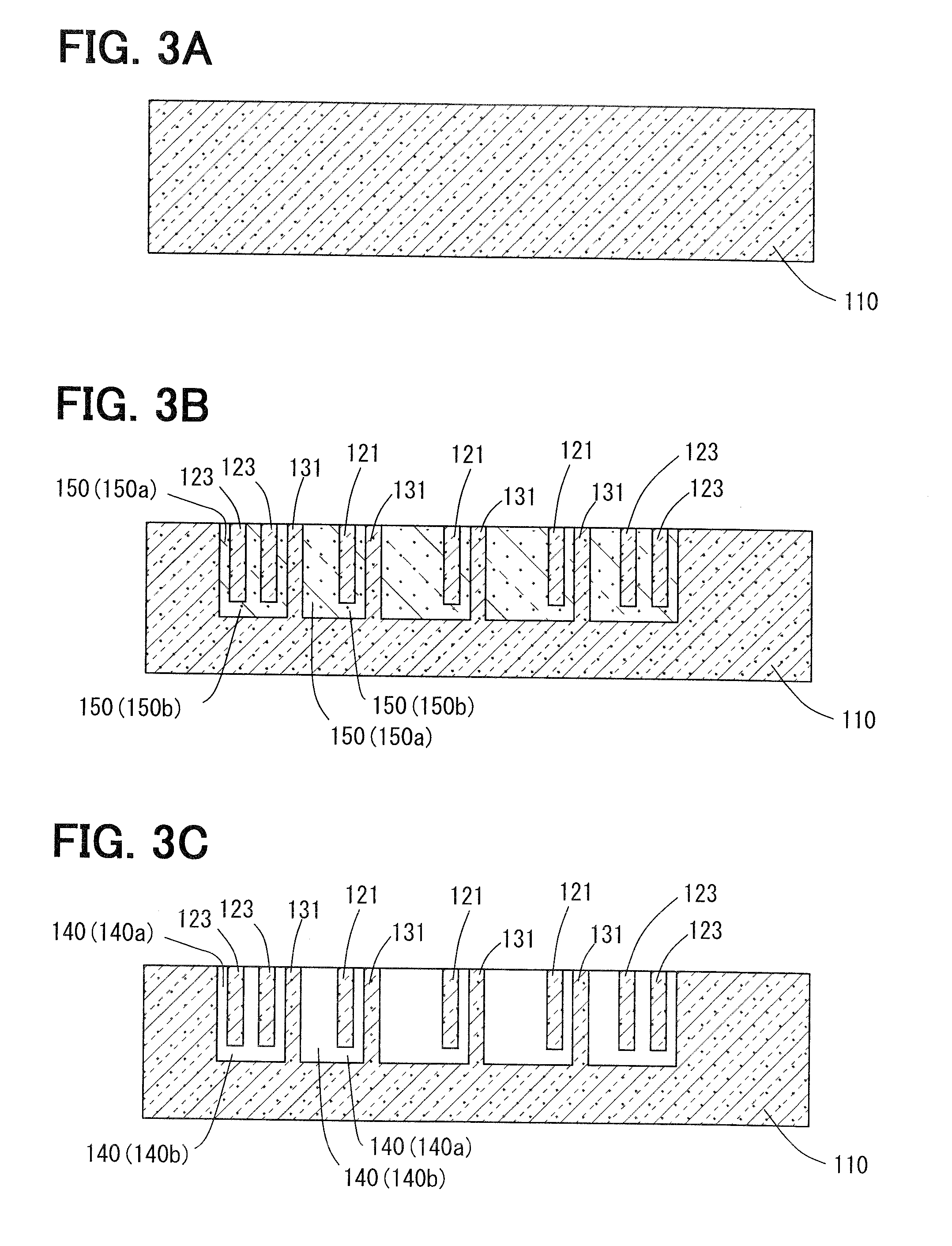
[0027]A physical quantity semiconductor sensor is manufactured by a manufacturing method according to an example embodiment. the sensor includes a movable portion, which is movable along with a predetermined direction according to a physical quantity applied to the sensor. Specifically, as shown in FIG. 1, the sensor is a capacitive acceleration sensor 100 for detecting acceleration. The sensor may be any sensor as long as the sensor includes a movable portion along with a predetermined direction according to a physical quantity. The sensor may be a MEMS device. For example, the sensor may be a capacitive angular speed sensor, a vibration sensor, a microphone, a micro scanner and the like.

[0028]As shown in FIGS. 1 and 2, the sensor 100 is made of a single crystal silicon substrate 110 having a movable portion and a fixed portion. Here, the substrate 110 is a single, i.e., one integrated substrate. Thus, the movable portion and the fixed portion are integrally formed in the single cr...


PUM

PropertyMeasurementUnit
Depthaaaaaaaaaa

Abstract

A manufacturing method of a semiconductor device includes: irradiating a laser beam on a single crystal silicon substrate, and scanning the laser beam on the substrate so that a portion of the substrate is poly crystallized, wherein at least a part of a poly crystallized portion of the substrate is exposed on a surface of the substrate; and etching the poly crystallized portion of the substrate with an etchant. In this case, a process time is improved.

Description

CROSS REFERENCE TO RELATED APPLICATION[0001]This application is based on Japanese Patent Application No. 2009-184969 filed on Aug. 7, 2009, the disclosure of which is incorporated herein by reference.FIELD OF THE INVENTION[0002]The present invention relates to a manufacturing method of a semiconductor device including an etching step.BACKGROUND OF THE INVENTION[0003]Conventionally, JP-A-2008-264902 teaches a manufacturing method of a semiconductor device including an etching step for etching single crystal silicon.[0004]In the above manufacturing method, a SOI substrate including a base layer made of single crystal silicon, an intermediate layer made of oxide silicon and an upper layer made of single crystal silicon, which are stacked in this order, is used. An oxide film patterned on the surface of the upper layer is used as a mask. Then, the upper layer is etched so as to reach the intermediate layer. Then, the intermediate layer is etched with using an etchant such as HF acid.[00...

Claims


Application Information

Patent Timeline
IPC IPC(8): H01L21/302B23K26/00B81C1/00G01P15/125H01L29/84
CPCB81B2203/0136B81B2203/0315B81C1/00484B81C1/005H01L21/32137H01L21/02532H01L21/02675H01L21/02691B81C2201/0143
Inventor KANAMORI, KATSUHIKOTOTOKAWA, MASASHITANAKA, HIROSHI
Owner DENSO CORP
Why Eureka
Try Eureka