Field effect transistor, semiconductor device and semiconductor device manufacturing method

a field effect transistor and semiconductor technology, applied in the direction of transistors, semiconductor devices, electrical apparatus, etc., can solve the problems of uneven display in the display, overlapping of the gate electrode and the source/drain electrode, and slow circuit operation, so as to improve interfacial strength, reduce contact resistance, and improve the effect of interfacial strength

Inactive Publication Date: 2011-03-03
IDEMITSU KOSAN CO LTD
View PDF10 Cites 49 Cited by
  • Summary
  • Abstract
  • Description
  • Claims
  • Application Information

AI Technical Summary

Benefits of technology

[0034]There are no particular restrictions on the material for forming each of the source electrode and the drain electrode. Materials which are commonly used can be arbitrary used as far as they do not impair the advantageous effects of the invention. For example, transparent electrodes such as indium tin oxide (ITO), indium zinc oxide, ZnO and SnO2, metal electrodes such as Al, Ag, Cr, Ni, Mo, Au, Ti, Ta, Cu, W and Nb or metal electrodes of alloys containing these metals can be used. In addition, it is preferred that two or more of these be stacked to decrease contact resistance or to improve interfacial strength. Further, in order to decrease the contact resistance of the source electrode and the drain electrode, the interface between the semiconductor and the electrode is subjected to a plasma treatment, an ozone treatment or the like to adjust the resistance.
[0035]There are no particular restrictions on the material for forming the gate electrode. Materials which are commonly used can be arbitrary used as far as they do not impair the advantageous effects of the invention. For example, transparent electrodes such as indium tin oxide (ITO), indium zinc oxide, ZnO and SnO2, metal electrodes such as Al, Ag, Cr, Ni, Mo, Au, Ti, Ta, Cu, W and Nb, or metal electrodes of alloys containing these metals can be used. In addition, it is preferred that two or more of these be stacked to decrease contact resistance or to improve interfacial strength. When the gate electrode is heated, as the material of the gate electrode, a material which is easy to be heated, i.e., one having a low reflectance and a high thermal absorption rate, or the like, is desirable. For that purpose, metals or alloys are preferable. It is also preferable to lower the reflectance by subjecting it to a surface treatment.
[0036]There are no particular restrictions on the material for forming the gate insulating film. Materials which are commonly used can be arbitrary used as far as they do not impair the advantageous effects of the invention. For example, oxides such as SiO2, SiNx, Al2O3, Te2O5, TiO2, MgO, ZrO2, CeO2, K2O, Li2O, Na2O, Rb2O, Sc2O3, Y2O3, Hf2O3, CaHfO3, PbTi3, BaTa2O6, SrTiO3, AlN or the like may be used. Of these, SiO2, SiNx, Al2O3, Y2O3, Hf2O3 and CaHfO3 are preferably used, with SiO2, SiNx, Y2O3, Hf2O3 and CaHfO3 being more preferable. The oxygen number of these oxides may not necessarily coincide with the stoichiometrical ratio (for example, they may be SiO2 or SiOx).
[0037]The gate insulating film may be a stack structure in which two or more different insulating films are stacked. The gate insulating film may be crystalline, polycrystalline or amorphous. It is preferred that the gate insulating film be polycrystalline or amorphous since it can be produced easily on the industrial scale.
[0038]The crystalline oxide in the semiconductor layer preferably comprises at least In. If it contains an indium element, the content of the indium element relative to all atoms excluding oxygen is preferably 87 at % or more and 100 at % or less, and more preferably 90 at % or more and 99 at % or less. If the content of the indium element is less than 87 at %, the crystallization temperature of the crystalline layer may be increased to cause crystals to be ununiform, or the mobility of the resulting thin film transistor may be lowered.
[0039]It is more preferred that the crystalline oxide be a composite oxide which contains two or more elements other than oxygen.

Problems solved by technology

If the overlapping is larger than 3.0 μm, the parasitic resistance is increased to cause the circuit operation to be slow.
If the gate electrode is not produced such that it is self-aligned with the source / drain electrodes, the overlapping of the gate electrode and the source / drain electrode may vary due to an error in mask alignment.
If the overlapping of the gate electrode and the source / drain electrodes varies, the capacitance between them may vary, thereby causing uneven display in a display.

Method used


Image

  • Field effect transistor, semiconductor device and semiconductor device manufacturing method
  • Field effect transistor, semiconductor device and semiconductor device manufacturing method
  • Field effect transistor, semiconductor device and semiconductor device manufacturing method

Examples


embodiment 1

[Bottom-Gate Type Self-Aligned Transistor]

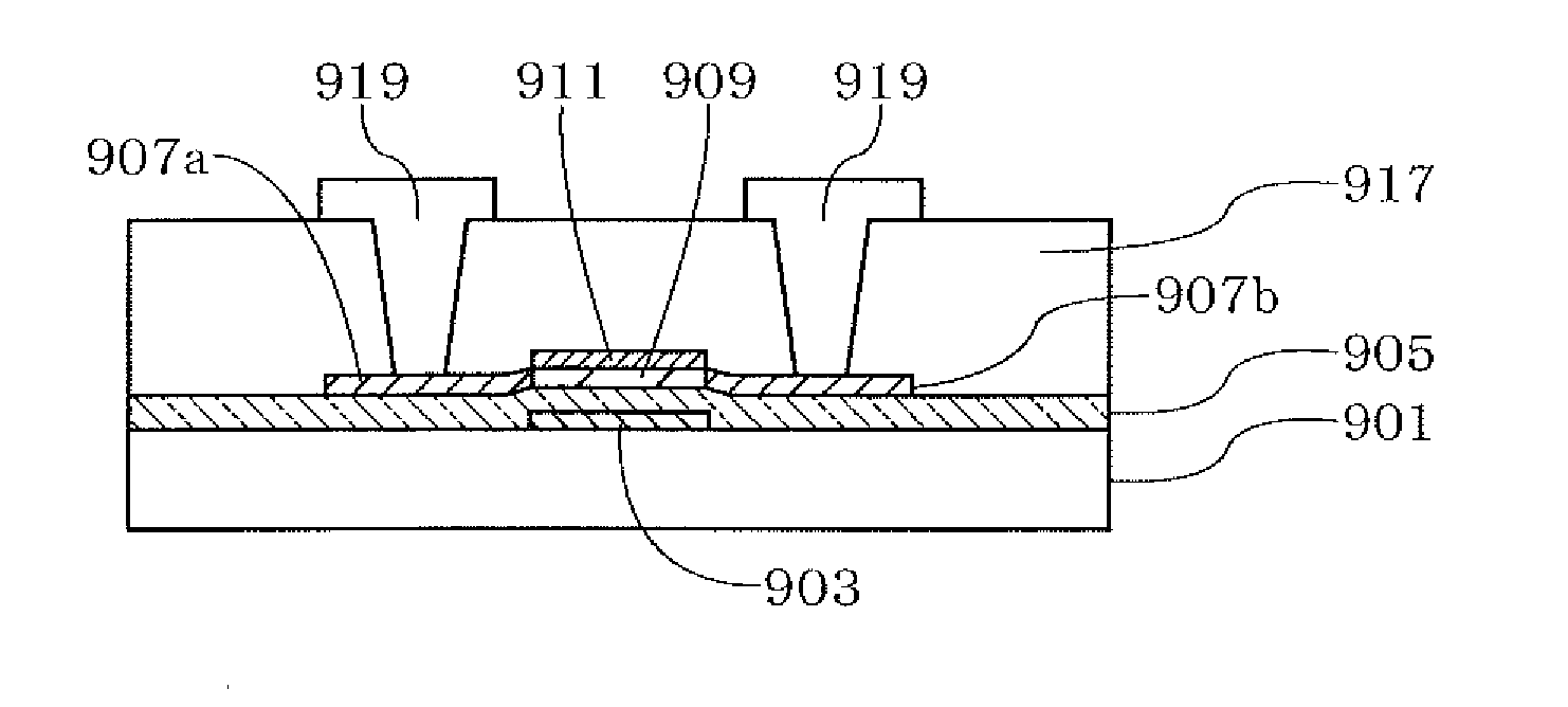
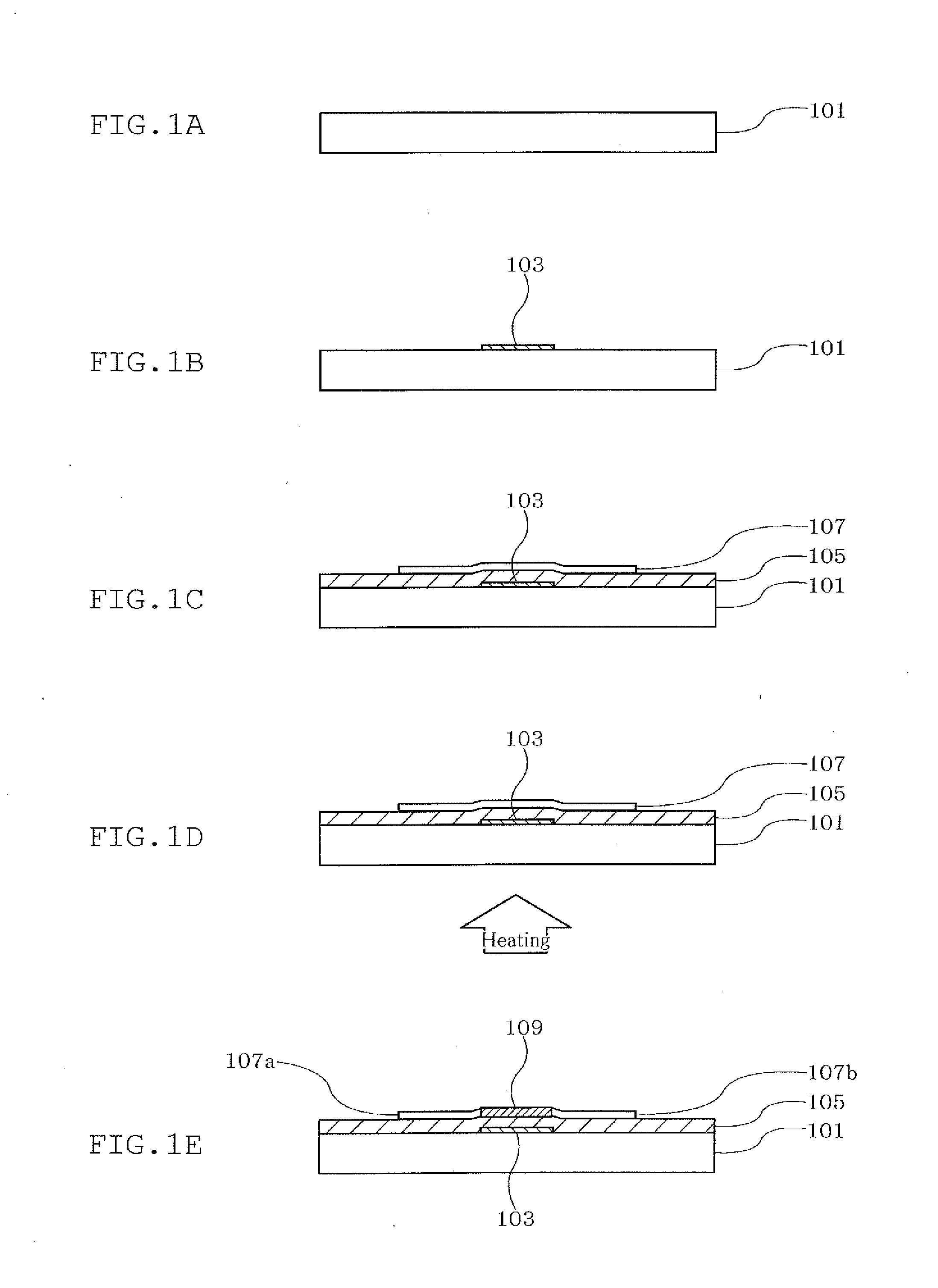
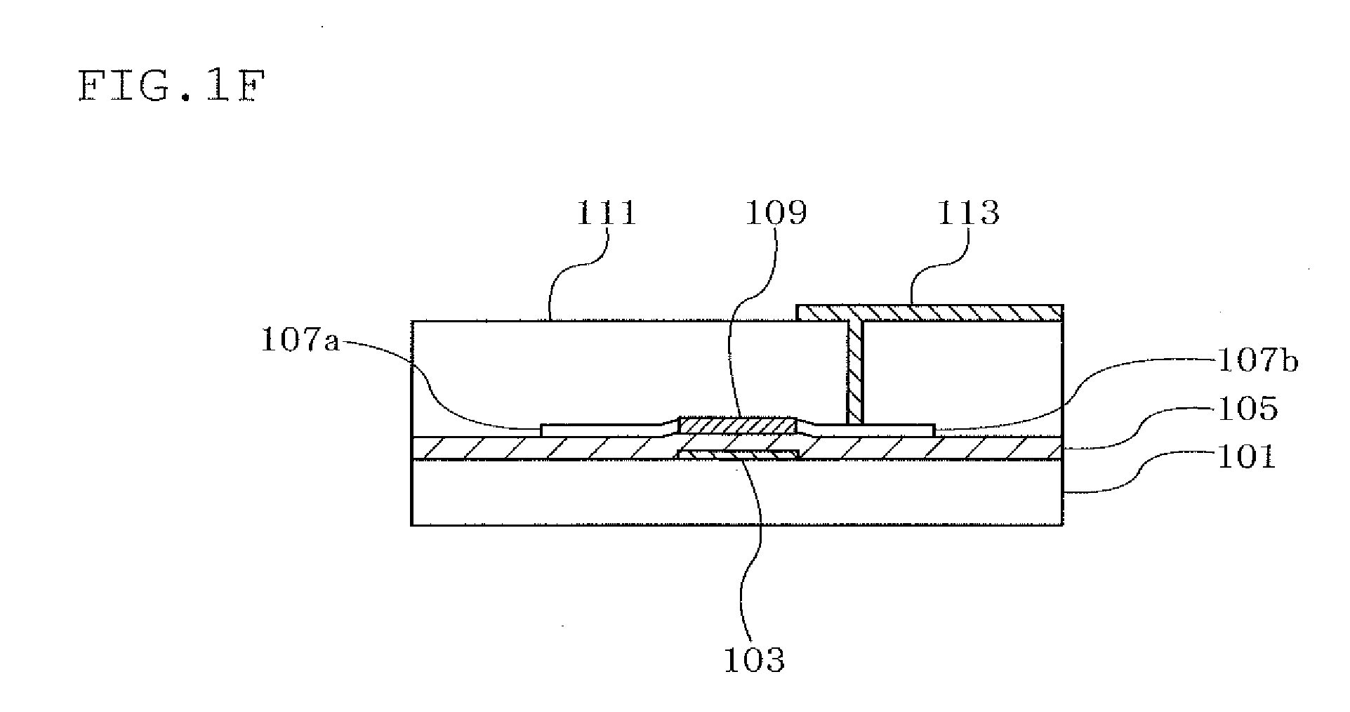
[0165]In this embodiment, by heating the gate electrode, a part of the conductive amorphous oxide film which overlaps the gate electrode is allowed to be semiconductive (crystallized) to form a semiconductor layer. A part which does not overlap the gate electrode retains its conductivity and becomes the source / drain electrodes. As a result, a self-aligned field effect transistor can be formed. The semiconductor layer and the source / drain electrodes have the same composition.

[0166]FIGS. 1A to F each show a step of the method for producing a transistor of Embodiment 1.

(1) Substrate

[0167]A substrate 101 provided with an undercoating film (not shown) is prepared (FIG. 1A).

[0168]As the undercoating film, a single layer of an insulating layer such as a silicon oxide film, a silicon nitride film, a silicon oxynitride film (SiOxNy) (x>y), a silicon nitroxide film (SiNxOy) (x>y) or the like or a stack of these films can be used. The undercoating film...

embodiment 2

[Bottom-Gate Type Self-Aligned Transistor]

[0194]This embodiment differs from Embodiment 1 in that the transistor having the same shape as that of Embodiment 1 is produced by photolithography using the gate electrode as a mask. In this embodiment, the gate electrode is not heated. Also in this embodiment, the semiconductor layer and the source / drain electrodes have the same composition.

[0195]FIGS. 2A to 2E each show a step of the method for producing a transistor of Embodiment 2.

[0196]In the same manner as in Embodiment 1, on a substrate 201, a gate electrode 203, a gate insulating film 205 and an amorphous oxide film 207 are formed (FIG. 2A). Further, a resist 215 is applied (FIG. 2B). Subsequently, using a gate electrode 203 as a mask, light is irradiated from below the gate electrode 203, and the resist 215 is developed and removed, whereby the part above the gate electrode 203 is opened (FIG. 2C).

[0197]Subsequently, an amorphous oxide film 207 in the opening of the resist 201 is ...

embodiment 3

[Bottom-Gate Type Self-Aligned Transistor]

[0199]In this embodiment, a transistor is formed by a lift off process by using a gate electrode as a mask.

[0200]FIGS. 3A to F are each a view showing a step of the method for producing a transistor of Embodiment 3.

[0201]As in the case of Embodiment 1, on a substrate 301, a gate electrode 303, a gate insulating film 305 and an amorphous oxide film 307 are formed (FIG. 3A). Subsequently, the amorphous oxide film 307 is allowed to be semiconductive (crystallized) 309 (FIG. 3B). Allowing the amorphous oxide film to be semiconductive can be conducted by annealing by means of an electric furnace or the like. The relationship between the temperature and the time during the annealing is shown in FIG. 10. Based on this relationship, an appropriate treatment temperature and an appropriate treatment time can be selected. Thereafter, a resist 315 is applied, and using the gate electrode 303 as a mask, light is irradiated from below the gate electrode 3...


PUM


Abstract

A field effect transistor including a source electrode 107a, a drain electrode 107b, a gate electrode 103, an insulating film 105 and a semiconductor layer 109 containing a crystalline oxide, wherein the source electrode 107a and the drain electrode 107b are self-aligned with the gate electrode 103 with the insulating film 105 therebetween.

Description

TECHNICAL FIELD[0001]The invention relates to a field effect transistor having an oxide film as a semiconductor layer and a production method thereof, and to a semiconductor device provided with the field effect transistor. In particular, the invention relates to a field effect transistor which has transistor properties capable of being applied to displays or the like.[0002]A field effect transistor is a device which is widely used as a unit electronic element of a semiconductor memory integrated circuit, a high-frequency signal amplification element, a liquid crystal driving element or the like. It is an electronic device which is most practically used in recent years.[0003]Of field effect transistors, with a significant development in displays in recent years, not only in liquid crystal displays (LCD) but also in various displays such as electroluminescence displays (EL) and field emission displays (FED), a thin film transistor (TFT) has been widely used as a switching element for...

Claims


Application Information

Patent Timeline
Patent Type & Authority Applications(United States)
IPC IPC(8): H01L29/786H01L21/44
CPCH01L29/7869
Inventor YANO, KOKIINOUE, KAZUYOSHITOMAI, SHIGEKAZU
Owner IDEMITSU KOSAN CO LTD
Why Eureka
Try Eureka