Method for performing electron beam lithography

a technology electron beam, which is applied in the field of electron beam lithography, can solve the problems of reducing the necessary exposure time below a certain limit of any given electron beam lithography system, limiting the scanning speed of the lithography system, etc., and achieves the effect of reducing, alleviating or eliminating one, and sufficient tim

Active Publication Date: 2011-03-03
NIL TECH APS (DK)
View PDF4 Cites 29 Cited by
  • Summary
  • Abstract
  • Description
  • Claims
  • Application Information

AI Technical Summary

Benefits of technology

[0007]Accordingly, the invention preferably seeks to mitigate, alleviate or eliminate one or more of the above mentioned disadvantages singly or in any combination. In particular, it may be seen as an object of the prese...

Problems solved by technology

This necessitates quite precise knowledge or feedback about the actual position of the beam, which, in turn, sets a limit to the scanning speed of the lithography system.
This makes it very critical...

Method used


Image

  • Method for performing electron beam lithography
  • Method for performing electron beam lithography
  • Method for performing electron beam lithography

Examples


Embodiment Construction

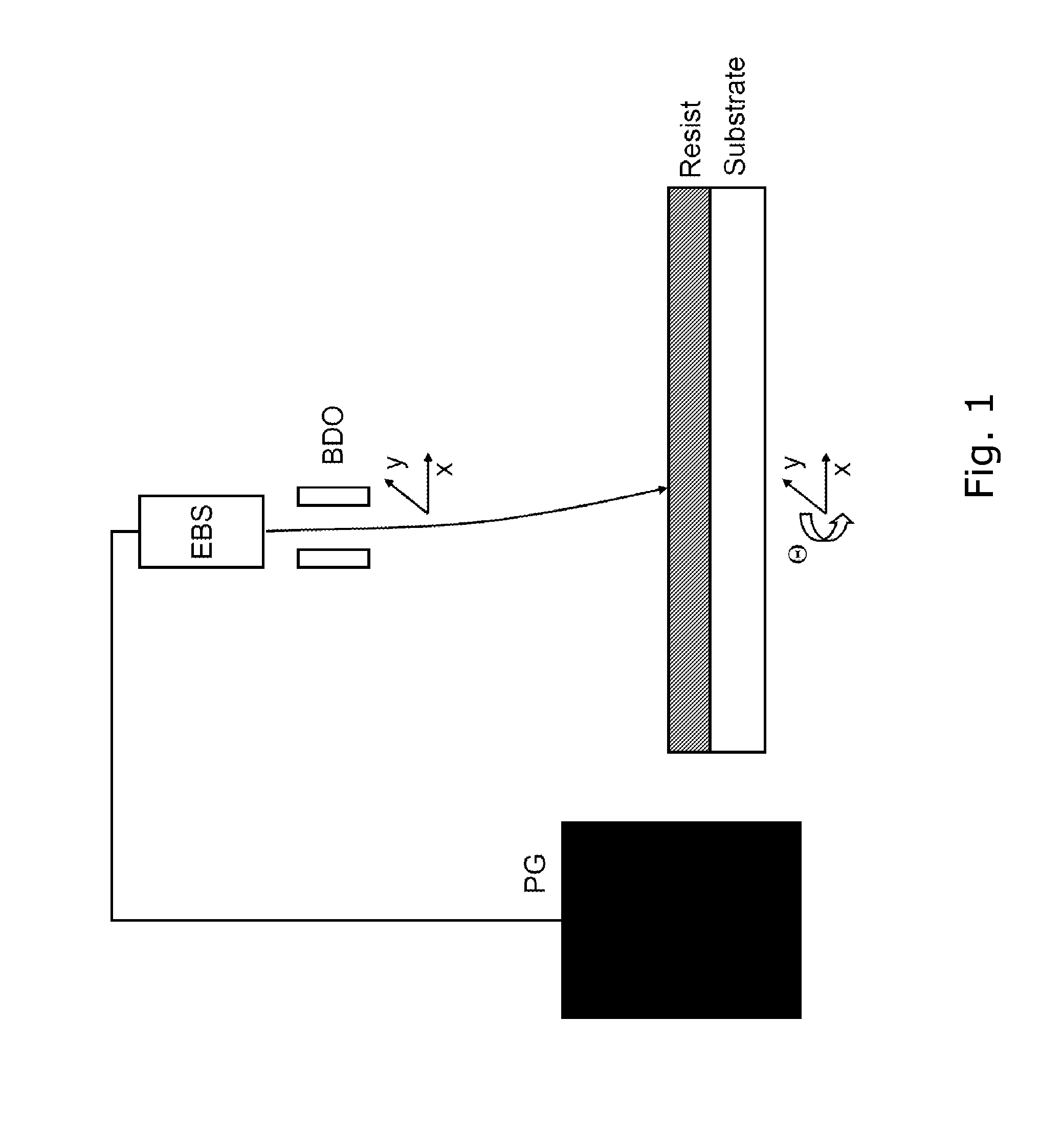
[0052]FIG. 1 is a schematic drawing of an electron beam source over a substrate with an energy sensitive resist.

Annotations used in FIG. 1:

PG: Pattern Generator

[0053]EBS: Electron beam source

BDO: Beam deflection optics

[0054]The electron beam moves relative to the substrate, either by moving the beam, moving the substrate or both simultaneously.

[0055]In order to perform electron beam lithography (EBL), there is provided a substrate with an energy sensitive resist with a threshold dose / energy, also known as clearing dose, saturation dose / energy, on a surface of the substrate.

[0056]Additionally, an electron beam source (EBS) with beam deflecting optics (BDO) is provided so that the EBS is capable of emitting an electron beam towards the energy sensitive resist, preferably with a nano-meter scale precision.

[0057]Next, there is performed a relative displacement of the electron beam across the substrate a first plurality of times so as to form a first pattern (P1) on the substrate, th...


PUM


Abstract

The present invention relates to a method for performing high speed electron beam lithography (EBL). An electron beam source (EBS), capable of emitting an electron beam towards the energy sensitive resist, forms a first pattern (P1) on the substrate, the first pattern defining a first direction (D1) on the substrate. The electron beam source then forms a second pattern (P2) on the substrate. The energy and/or dose delivered to the energy sensitive resist during the exposure of the first and the second pattern is dimensioned so that the threshold dose/energy of the energy sensitive resist is reached on the overlapping portions of the first and the second patterns (P1, P2). The invention provides a high speed technique for the production of substrates with high quality developed patterns, e.g. hole or dot arrays, by electron beam lithography. Each hole or dot may be defined by the mutually overlapping portions of the first and second pattern, e.g. exposed lines forming a grid, instead of addressing each dot or hole separately.

Description

FIELD OF THE INVENTION[0001]The present invention relates to a method for performing electron beam lithography. The invention also relates to a corresponding computer program product.BACKGROUND OF THE INVENTION[0002]Electron-beam lithography has developed after the limit was reached in optical lithography as regards the smallest spot that could reasonably be formed by optical means. Electron-beam lithography makes it possible to record significantly smaller pits / grooves on an energy sensitive resist on a wafer for optical or electronic applications.[0003]US2003155532 discloses a device for electron-beam lithography wherein very small pits can be written, using a small beam intensity, by exposing each pit several times during writing thereby avoiding the mutual repulsion between the electrons setting an upper limit for electron density in the beams. A row of electron beams is arranged in the longitudinal direction of the track. Each beam from the row of beams can be controlled, eithe...

Claims


Application Information

Patent Timeline
IPC IPC(8): G03F7/20G21G5/00
CPCB82Y10/00H01J37/3174B82Y40/00G03F7/203H01L21/0275
Inventor NIELSEN, THEODOR KAMPBILENBERG, BRIANSHI, PEIXIONG
Owner NIL TECH APS (DK)
Why Eureka
Try Eureka