

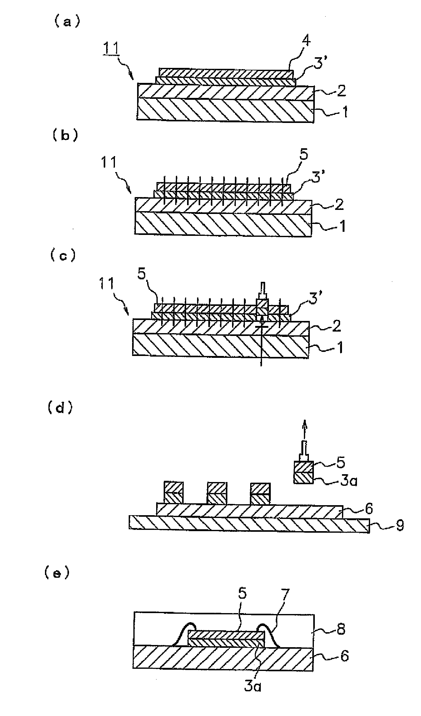
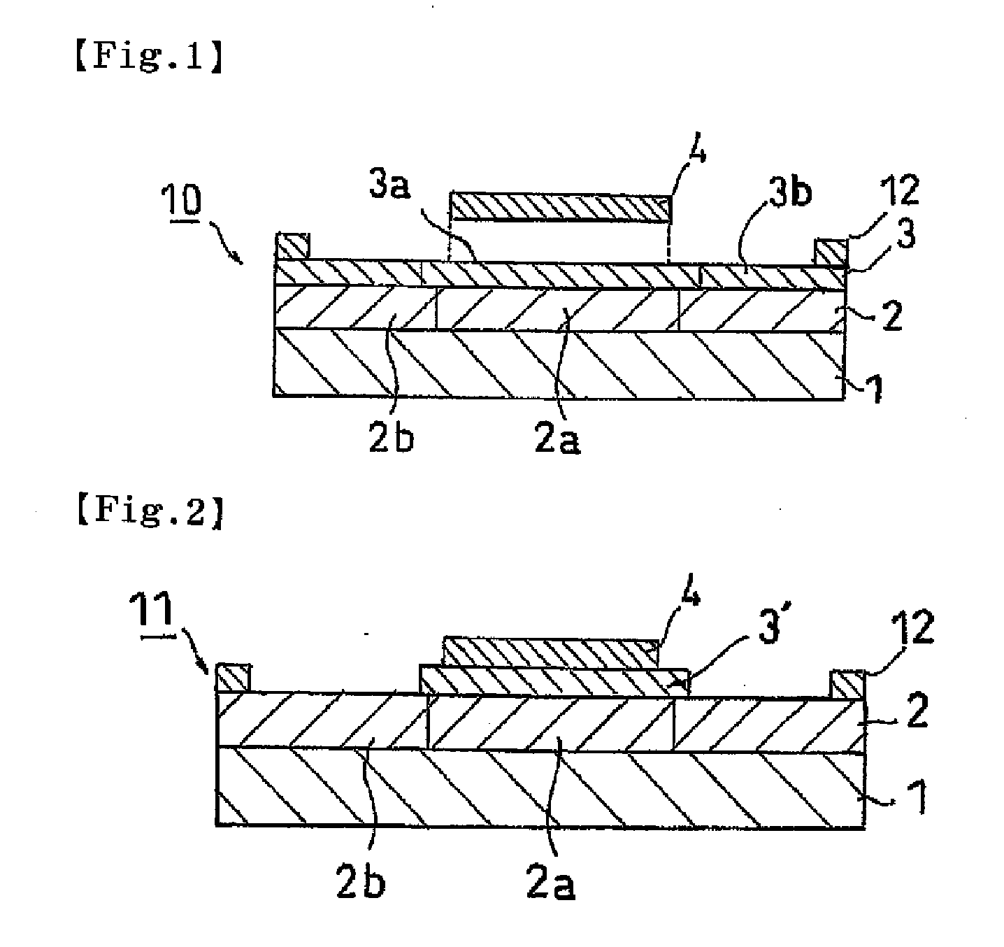
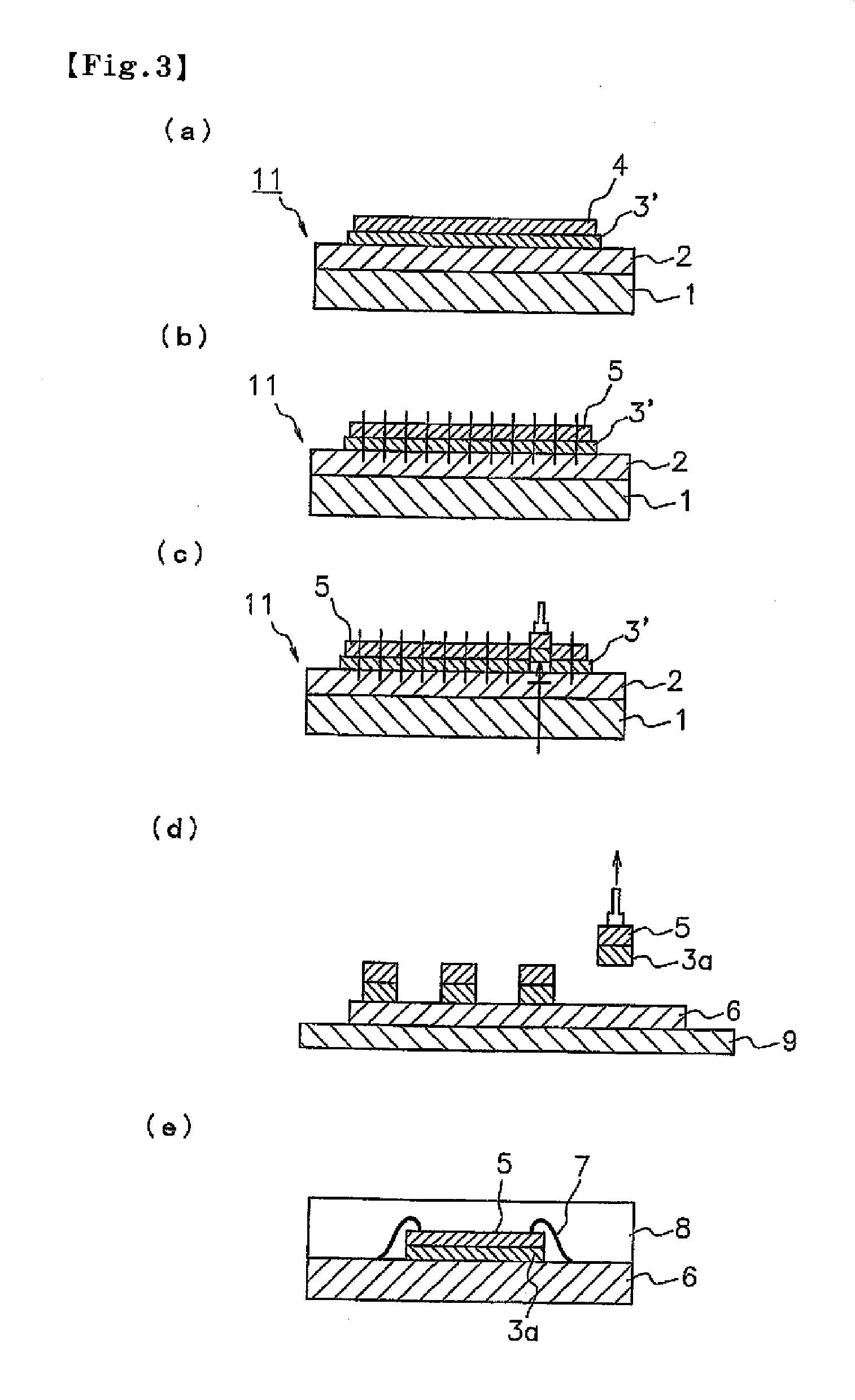
Dicing/die bonding film
a die-bonding film and die-bonding technology, applied in film/foil adhesives, solid-state devices, synthetic resin layered products, etc., can solve the problems of difficult uniformity of adhesive layers, long time, special apparatus, etc., and achieve easy peeling, excellent pickup properties, and reduced yield ratio
- Summary
- Abstract
- Description
- Claims
- Application Information
AI Technical Summary
Benefits of technology
Problems solved by technology
Method used
Image

Examples
example 1
[0114]
[0115]To a reaction vessel equipped with a condenser, a nitrogen introducing tube, a thermometer and a stirrer, 86.4 parts of 2-ethylhexyl acrylate (hereinafter referred to as “2EHA”), 13.6 parts of 2-hydroxyethyl acrylate (hereinafter referred to as “HEA”), 0.2 part of benzoyl peroxide and 65 parts of toluene were charged and then polymerized in a nitrogen gas flow at 61° C. for 6 hours to obtain an acrylic polymer A. The content of HEA was adjusted to 20 mol %.
[0116]To this acrylic polymer A, 14.6 parts (80 mol % based on HEA) of 2-methacryloyloxyethyl isocyanate (hereinafter referred to as “MOI”) was added and the mixture was subjected to an addition reaction treatment in an air flow at 50° C. for 48 hours to obtain an acrylic polymer A′.
[0117]Next, to 100 parts of the acrylic polymer A′, 8 parts of a polyisocyanate compound (trade name “CORONATE L”, manufactured by Nippon Polyurethane Industry Co., Ltd.) and 5 parts of a photopolymerization initiator (trade name “IRGACURE ...
examples 2 to 10
[0128]In Examples 2 to 10, each dicing die-bonding film was manufactured in the same manner as in Example 1, except that the composition and the content were changed to those shown in Table 1.
TABLE 1Hydroxyl group-IsocyanateCrosslinkingPhotopoly-containing monomercompoundagentmerization2EHAHEA4HBAMOIAOIC / LC2030initiatorExample 186.413.6 (20)—14.6 (80)—8—5Example 293.5 6.6 (10)— 7.9 (90)—8—5Example 378.721.3 (30)—22.7 (80)—8—5Example 486.413.6 (20)—12.3 (70)—8—5Example 584—16 (20)14.2 (80)—8—5Example 686.413.6 (20)——13.4 (80)8—5Example 786.413.6 (20)—14.6 (80)—4—5Example 886.413.6 (20)—14.6 (80)—16—5Example 986.413.6 (20)—14.6 (80)——85Example 1072.6 27.4 (37.5)—29.3 (80)—8—5The numerical values in parentheses represent “mol”, while the numerical values in parentheses in MOI and AOI represent “molar ratio” to HEA or 4HBA.
[0129]The meanings of abbreviations described in Table 1 and Table 2 mentioned hereinafter are as follows.[0130]2EHA: 2-ethylhexyl acrylate[0131]HEA: 2-hydroxyethyl a...
PUM
| Property | Measurement | Unit |
|---|---|---|
| temperature | aaaaa | aaaaa |
| thickness | aaaaa | aaaaa |
| thickness | aaaaa | aaaaa |
Abstract
Description
Claims
Application Information