Lateral Insulated Gate Bipolar Transistors (LIGBTS)

a bipolar transistor and insulated gate technology, applied in the field of lateral insulated gate bipolar transistors (ligbts), can solve the problems of reducing the gain of the above pnp transistors, not always being the case, and reducing the charge injection region, so as to increase the switching speed, reduce the gain of the above pnp transistor, and increase the switching speed

Inactive Publication Date: 2011-03-10
POWER INTEGRATIONS INC
View PDF3 Cites 46 Cited by
  • Summary
  • Abstract
  • Description
  • Claims
  • Application Information

AI Technical Summary

Benefits of technology

[0017]The peak doping concentration (i.e., dopant concentration) lower than about 1×10¹⁹ / cm3 (or, more preferably, lower than about 1×10¹⁸ / cm3) as defined above may be advantageous for reducing the gain of a lateral pnp transistor (e.g. as shown in FIG. 2) and / or of a vertical pnp transistor (e.g. a first vertical pnp transistor as shown in FIG. 2 with the collector connected to the source / cathode, or as shown outside the thyristor in FIG. 33) of the LIGBT to increase switching speed by reducing plasma build-up as described herein. Alternatively or additionally this arrangement may lead to a reduction in the current gain of the second vertical pnp transistor shown for example in FIGS. 28-33, and therefore may minimise the effect of the break-over (i.e. the activation) and / or the latch-up of the parasitic thyristor as described for example in relation to the eighth to thirteenth aspects. Preferably, the above peak doping concentration of the first contact region is greater than about 5×10¹⁷ / cm3 and / or is lower than a dopant concentration of the second contact region.
[0047]According to a seventh aspect of the present invention, there is provided a method of increasing switching speed of an LIGBT, the LIGBT comprising: a first contact region of a first conductivity type as a charge injection semiconductor region; a second contact region of a first conductivity type; a source region of a second, opposite conductivity type located within a well region of first conductivity type and connected electrically to said second contact region; a lateral drift region of the second conductivity type placed between the said well region and said first contact region, said lateral drift region to be depleted of mobile carriers during an off-state blocking mode of the LIGBT and able to conduct charge during on-state conducting mode of the LIGBT; and an insulated gate placed above and in direct contact to said well region, said insulated gate to control the charge in a channel region between said lateral drift region and said source region of said second conductivity type and to thereby control flow of charge within the said drift region, the method comprising: forming a buried floating semiconductor region below said charge injection semiconductor region and adjacent said lateral drift region, the buried floating semiconductor region being of the second conductivity type and more highly doped than said lateral drift region.

Problems solved by technology

More specifically, charge injection from the charge injection region may be reduced due to the presence of the floating region due to decrease in injection efficiency and / or Auger recombination, and this may reduce the gain of the above pnp transistors.
(However, the latter may not always be the case, for example in some SOI and / or membrane technology embodiments described in this specification).

Method used


Image

  • Lateral Insulated Gate Bipolar Transistors (LIGBTS)
  • Lateral Insulated Gate Bipolar Transistors (LIGBTS)
  • Lateral Insulated Gate Bipolar Transistors (LIGBTS)

Examples


Embodiment Construction

[0104]The following describes arrangements falling within the broader aspects of the present invention summarised above, and more specific embodiments.

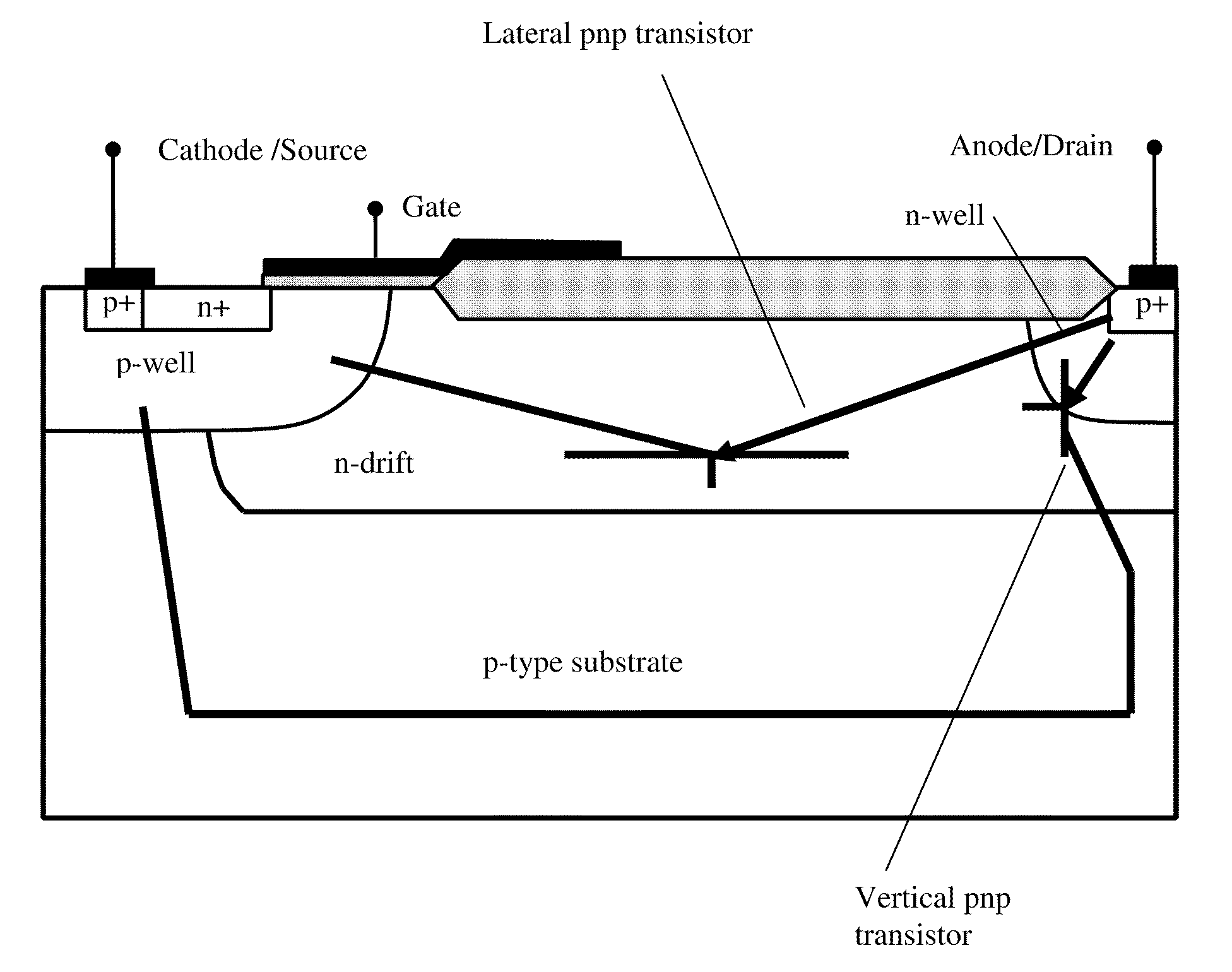
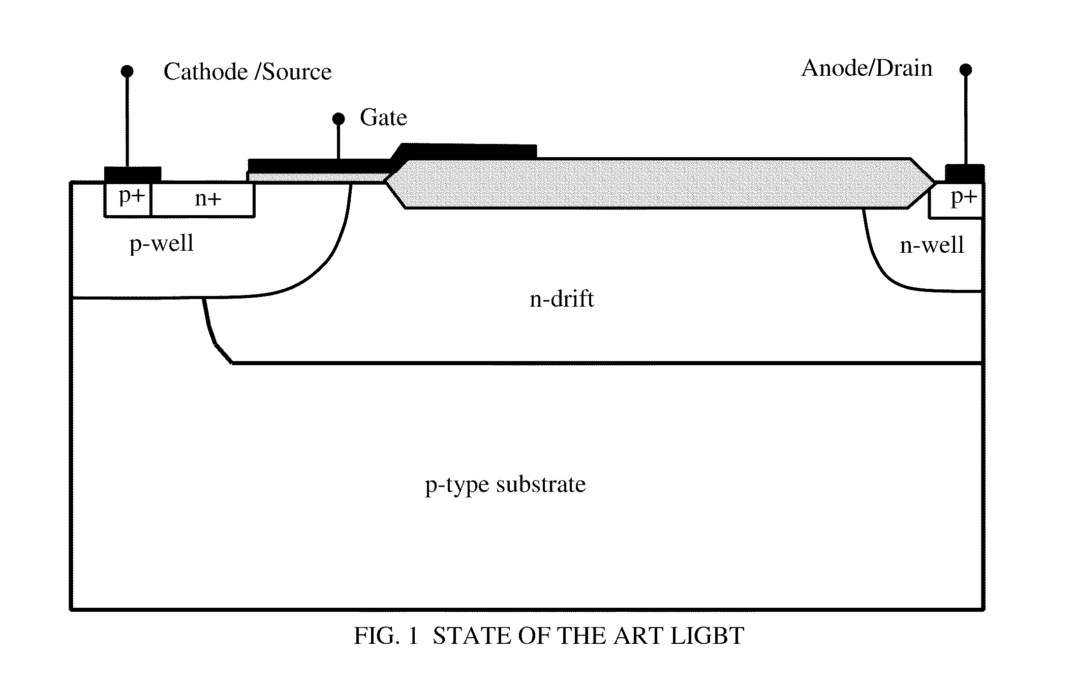
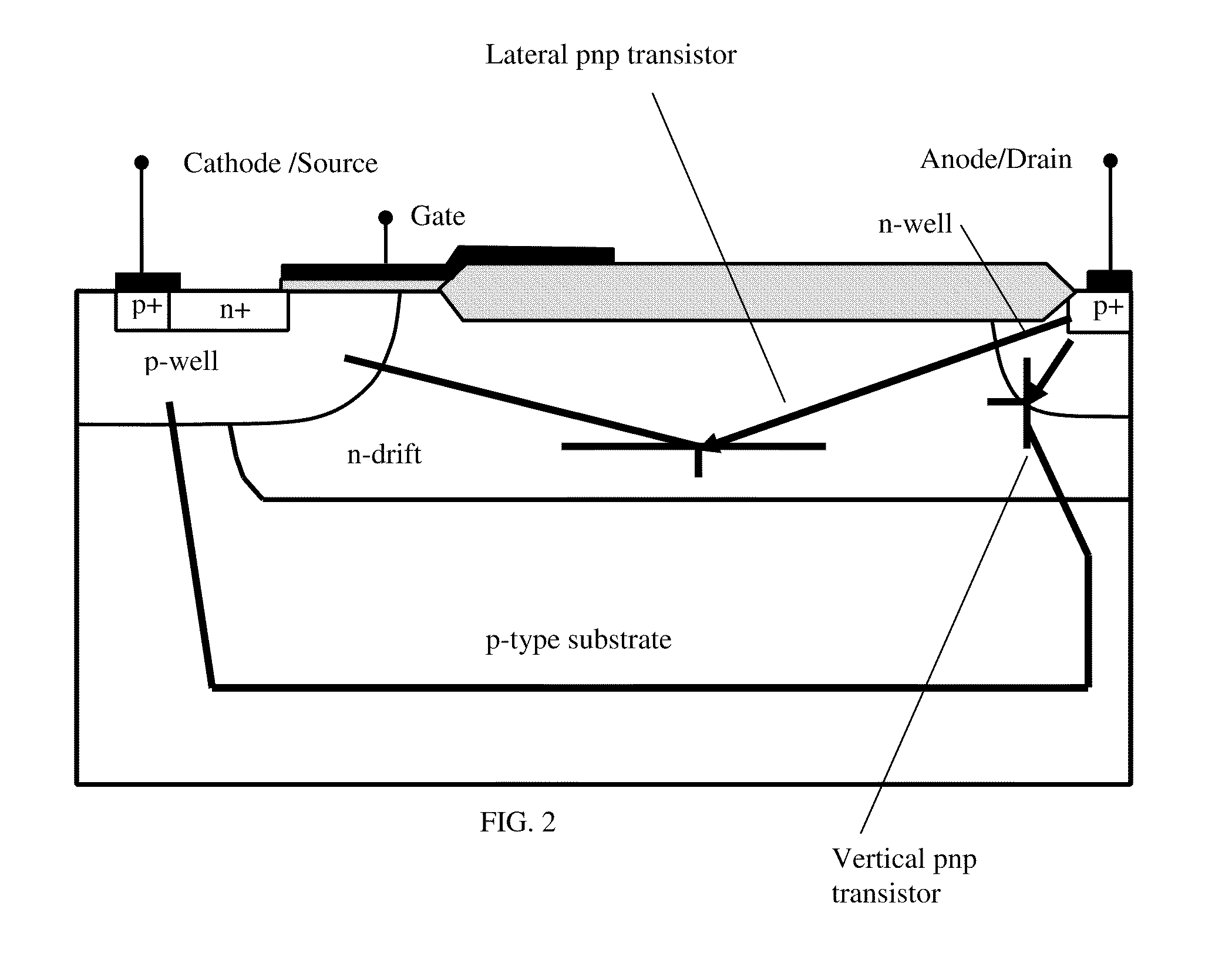
[0105]Embodiments are particularly concerned with high voltage semiconductor devices which can be used in power integrated circuits and have particular application to MOS-bipolar transistors.

[0106]An LIGBT embodiment includes relatively lowly doped, p type, transparent anode injectors and / or floating highly doped n+ layer at the surface or buried, adjacent to the anode region in order to reduce the gain of a pnp transistor (e.g., the vertical pnp transistor of FIG. 2 or first vertical transistor of FIG. 33) and hence increase the turn-off speed of the device. In one arrangement, e.g., the first arrangement, the doping of the p type injector is adjusted to control the injection efficiency of the anode junction and thus to reduce the amount of plasma injected into the device so as to increase the switching speed. The p type anode layer ...


PUM


Abstract

This invention generally relates to lateral insulated gate bipolar transistors (LIGBTs), for example in integrated circuits, methods of increasing switching speed of an LIGBT, a method of suppressing parasitic thyristor latch-up in a bulk silicon LIGBT, and methods of fabricating an LIGBT. In particular, a method of suppressing parasitic thyristor latch-up in a bulk silicon LIGBT comprises selecting a current gain αv for a vertical transistor of a parasitic thyristor of the LIGBT such that in at least one predetermined mode of operation of the LIGBT αv<1−αp where αp is a current gain of a parasitic bipolar transistor having a base-emitter junction formed by a Schottky contact between the a semiconductor surface and a metal enriched epoxy die attach.

Description

RELATED APPLICATIONS[0001]The present invention claims priority from U.S. Provisional Patent Application No. 61 / 240,780, filed 9 Sep. 2009.FIELD OF THE INVENTION[0002]The invention generally relates to lateral insulated gate bipolar transistors (LIGBTs), for example in integrated circuits, methods of increasing switching speed of an LIGBT, a method of suppressing parasitic thyristor latch-up in a bulk silicon LIGBT, and methods of fabricating an LIGBT.BACKGROUND TO THE INVENTION[0003]Power devices operated in integrated circuits typically operate with a voltage in the range 20V to 1.2 kV and typically higher than 30V or 50V or so. Power devices typically operate with a current in the range 10 mA to 50 A and typically higher than 0.1 A and smaller than 5 A. Such devices may also be referred to as “high voltage / power devices”. These devices are typically capable of delivering from a few mWatts to 1 Watt or even a few tens of Watts of power. Their application may range from domestic ap...

Claims


Application Information

Patent Timeline
Patent Type & Authority Applications(United States)
IPC IPC(8): H01L29/739H01L21/761H01L21/331
CPCH01L29/66325H01L29/7394H01L29/7393
Inventor UDREA, FLORINPATHIRANA, VASANTHATRAJKOVIC, TANYAUDUGAMPOLA, NISHAD
Owner POWER INTEGRATIONS INC
Why Eureka
Try Eureka