Measuring Apparatus, Measuring Coordinate Setting Method and Measuring Coordinate Number Calculation Method
a technology of measuring apparatus and measuring coordinates, applied in the direction of mechanical measuring arrangements, instruments, using mechanical means, etc., can solve the problems of huge manufacturing cost, inability to evaluate the assessment level of device fabrication over the entire surface of the wafer with high precision, and inability to quickly analyze the cause of failure, improve the performance of the device, and improve the accuracy of the effect of the devi
- Summary
- Abstract
- Description
- Claims
- Application Information
AI Technical Summary
Benefits of technology
Problems solved by technology
Method used
Image

Examples
embodiment 1
[0039]First, an electron microscope to measure dimensions of patterns formed on a device will be explained as embodiment 1.
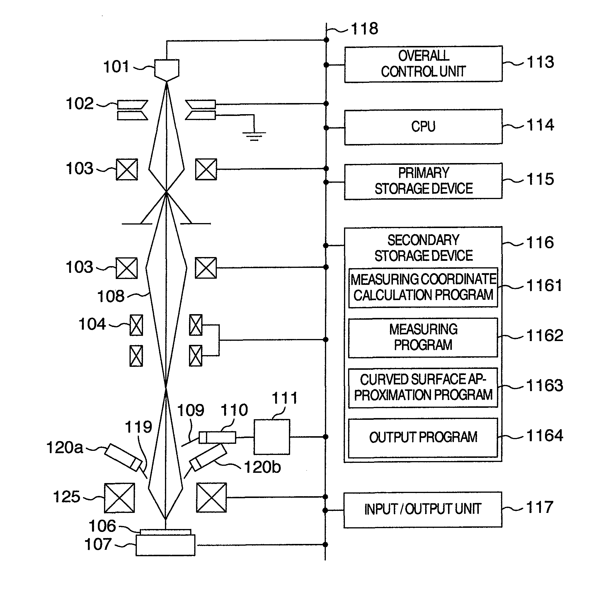
[0040]FIG. 1 shows an overview of an electron microscope as one example of a measuring apparatus of this invention. The electron microscope comprises an electron source 101 for generating primary electrons 108, an acceleration electrode 102 for accelerating the primary electrons, a focusing lens 103 for focusing the primary electrons, a deflector 104 for deflecting the primary electrons two-dimensionally and an object lens 105 for focusing the primary electrons onto a substrate 106 such as wafer. Denoted 107 is a drive stage on which the substrate 106 is mounted. Designated 110 is a detector that detects a secondary electron signal 109 coming out of the substrate 106. Denoted 120a and 120b are reflected electron detectors that each detect a reflected electron signal 119. In the figure, the two reflected electron detectors 120a, 120b are set to oppose each other ...
embodiment 2
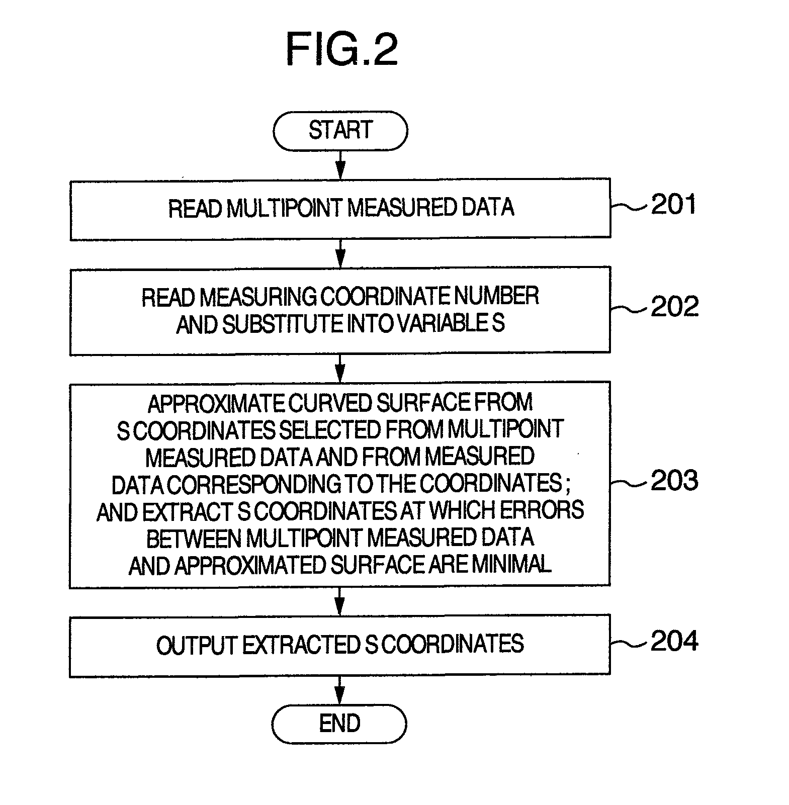
[0061]Therefore, with this tendency considered, the following measuring coordinate calculation program may be used as embodiment 2.
[0062]FIG. 17 shows an example flow chart that simplifies the measuring coordinate calculation program 1161. First, at step 271, a variable S and a variable T are arbitrarily set to randomly sample (S-T) coordinates. Next, step 272 arranges T coordinates along the outer circumference of the wafer to reduce approximation errors of the B-spline surface. Next, step 273 combines the (S-T) coordinates randomly sampled by step 271 with the T coordinates used for curved surface approximation at step 272, to calculate S coordinates.
[0063]FIG. 18 shows an example of wafer map of the (S-T) coordinates randomly sampled at step 271.
[0064]FIG. 19 shows an example of wafer map of the T coordinates that are deliberately placed along the outer circumference of the wafer at step 272.
[0065]FIG. 20 shows an example of table that shows how the dimension data measured at the...
embodiment 3
[0066]In embodiment 1 and 2, an appropriate number of measuring coordinates that does not impair the productivity is determined by taking into consideration the number of wafers manufactured daily at the device mass production plant, the number of measuring apparatus available at the plant and the processing speed of the measuring apparatus, and is substituted into the variable S at step 202. There are, however, cases where it is desired that the number of measuring coordinates be determined from the standpoint of reducing errors of the approximated values obtained through the curved surface approximation. In embodiment 3, therefore, a method of determining the number of measuring coordinates from the standpoint of reducing errors of approximated values will be explained.
[0067]FIG. 21 shows an example flow chart to evaluate errors for the variable S by preparing three kinds of multipoint measured data. This method evaluates errors by using a cross validation. First, step 281 reads t...
PUM
 Abstract
Description
Claims
Application Information
 - R&D
- Intellectual Property
- Life Sciences
- Materials
- Tech Scout
- Unparalleled Data Quality
- Higher Quality Content
- 60% Fewer Hallucinations
Browse by: Latest US Patents, China's latest patents, Technical Efficacy Thesaurus, Application Domain, Technology Topic, Popular Technical Reports.
© 2025 PatSnap. All rights reserved.Legal|Privacy policy|Modern Slavery Act Transparency Statement|Sitemap|About US| Contact US: help@patsnap.com