Methods for stable process in a reactive sputtering process using zinc or doped zinc target

a reactive sputtering and stable technology, applied in the direction of vacuum evaporation coating, electric discharge tube, coating, etc., can solve the problems of high cost of polysilicon with electron mobility above 50 cm/v-s, inability to meet large-area substrate applications, and inability to stabilize, etc., to achieve sufficient reduction or cleaning, the effect of reducing the redeposition of byproducts

Active Publication Date: 2011-03-31
APPLIED MATERIALS INC
View PDF100 Cites 3 Cited by
  • Summary
  • Abstract
  • Description
  • Claims
  • Application Information

AI Technical Summary

Benefits of technology

[0016]For example, the sputtering target should be set at a temperature lower than the substrate. Therefore, the reaction rate will be controlled through ion bombardment energy. During the deposition process, the ion bombardment is controlled so that the ion energy is high enough to minimize the redeposition of the byproduct, and low enough to avoid inducing other reactions on the target. During the cleaning process, the ion bombardment energy on the target should be high enough to remove the re-deposited byproduct but not enough to induce re-deposition on the substrate.
[0017]The reaction condition on the other exposed surface is mainly controlled by the temperature and exposure to the reactants. For a ZnON process, the temperature of the surface other than the substrate or target is set at a higher temperature than the target and at a lower temperature than the substrate. The higher temperature than the target enables the surfaces to have certain reduction reactions even though the ion bombardment energy is lower there. The lower temperature than the substrates make the deposition on the surface less oxidized than the film deposited on the substrate, so that sufficient reduction or cleaning takes place on the surfaces but not on the film at the substrate.

Problems solved by technology

Therefore, the cost of producing polysilicon with an electron mobility higher than 50 cm2 / V-s is very high and not suitable for large area substrate applications.
The hydrogen passivation, while helping the amorphous silicon achieve the desired mobility, may not be stable such that a TFT's threshold voltage may change with time under gate electrode voltage and under relatively high temperatures created by the device itself.

Method used


Image

  • Methods for stable process in a reactive sputtering process using zinc or doped zinc target
  • Methods for stable process in a reactive sputtering process using zinc or doped zinc target
  • Methods for stable process in a reactive sputtering process using zinc or doped zinc target

Examples


Embodiment Construction

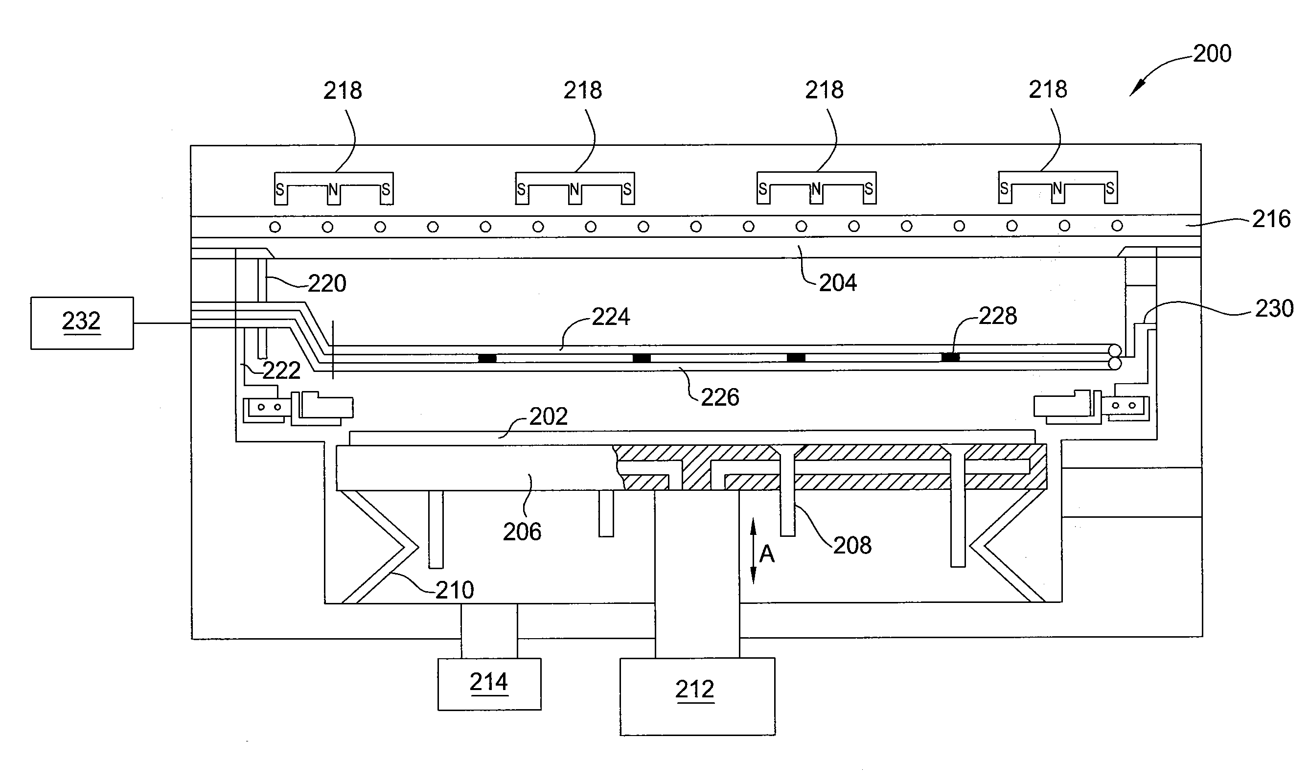
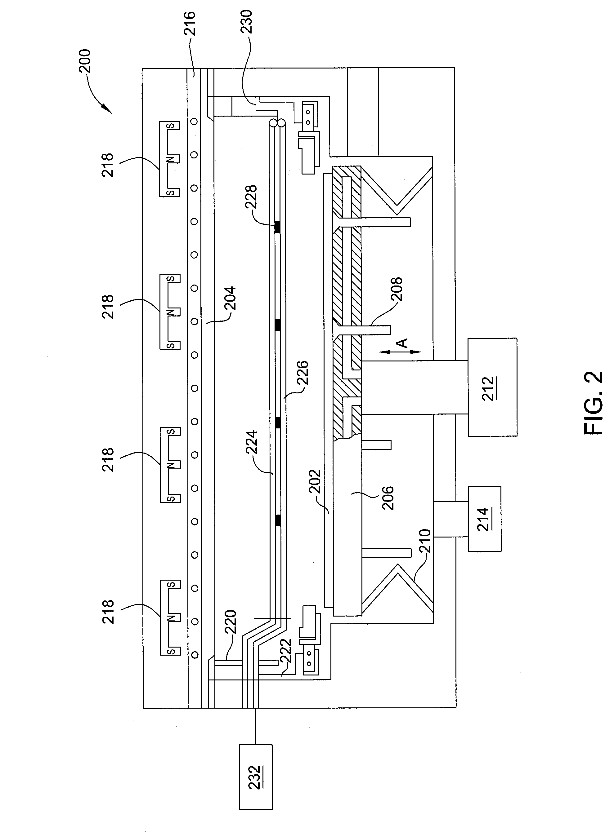
[0024]Embodiments disclosed herein generally relate to a method for seasoning a sputtering target and other exposed surfaces in-situ with a substrate to be processed. New semiconductor compounds containing oxygen, nitrogen, and an element such as zinc, cadmium, tin, indium, and gallium are beginning to replace silicon as the material for active channels in TFTs. The new semiconductor compounds may be deposited by a reactive sputtering process. During the sputtering process, reactive gas reacts with the metal from the sputtering target and deposits on the substrate. Some of the reactive gas may react at the surface and lead to a buildup of a compound at the target surface. Because oxygen and nitrogen are quite reactive, an oxide or nitride compound may develop at the target surface. The oxide or nitride may be removed by seasoning the sputtering target. The surface condition on the other exposed surfaces may be different both before and after the deposition process of the film deposi...


PUM

PropertyMeasurementUnit
temperaturesaaaaaaaaaa
temperatureaaaaaaaaaa

Abstract

Embodiments disclosed herein generally relate to a method for seasoning a sputtering target in-situ with a substrate to be processed. New semiconductor compounds containing oxygen, nitrogen, and an element such as zinc, cadmium, tin, indium, and gallium are beginning to replace silicon as the material for active channels in TFTs. The new semiconductor compounds may be deposited by a reactive sputtering process. During the sputtering process, reactive gas reacts with the metal from the sputtering target and deposits on the substrate. Some of the reactive gas may react at the surface and lead to a buildup of a compound at the target surface. Because oxygen and nitrogen are quite reactive, an oxide or nitride compound may develop at the target surface. The oxide or nitride may be removed by seasoning the sputtering target. The seasoning may occur while the substrate is within the processing chamber.

Description

CROSS-REFERENCE TO RELATED APPLICATIONS[0001]This application claims benefit of U.S. Provisional Patent Application Ser. No. 61 / 246,222 (APPM / 14377L), filed Sep. 28, 2009, which is herein incorporated by reference.BACKGROUND OF THE INVENTION[0002]1. Field of the Invention[0003]Embodiments disclosed herein generally relate to a method for seasoning a sputtering target in-situ with a substrate to be processed.[0004]2. Description of the Related Art[0005]The electron mobility of a semiconductor layer has a very strong effect on the speed of the device and the current which may be driven through the device. The higher the electron mobility, the faster the speed of the device and the higher the source-drain current under the same voltage. In recent years, amorphous silicon and polysilicon have been the semiconductor materials of choice for field effect transistors (FETs) such as thin film transistors (TFTs), for backplane to drive liquid crystal displays (LCDs), organic light emitting di...

Claims


Application Information

Patent Timeline
Patent Type & Authority Applications(United States)
IPC IPC(8): C23C14/34C23C14/06
CPCC23C14/0036C23C14/0676H01J37/3408C23C14/35C23C14/564C23C14/3492
Inventor YE, YAN
Owner APPLIED MATERIALS INC
Why Eureka
Try Eureka