Monolithic Integration of Photovoltaic Cells

a photovoltaic cell and monolithic technology, applied in the field of photovoltaic device manufacturing, can solve the problems of low conductivity of poor solar energy absorption of crystalline silicon, and inability to meet the requirements of light-weight thin film products, etc., to achieve the effect of high conductivity and facilitate monolithic series photovoltaic devices

Inactive Publication Date: 2011-04-14
OVSHINSKY TECH
View PDF10 Cites 3 Cited by
  • Summary
  • Abstract
  • Description
  • Claims
  • Application Information

AI Technical Summary

Benefits of technology

[0025]The transparent electrode is a transparent conductive material such as a conductive oxide. Embodiments of transparent conductive materials include tin oxide (SnO2), indium oxide (In2O3), ITO (indium tin oxide), zinc oxide (ZnO), zinc tin oxide (ZnSnO3, Zn2SnO4), and cadmium tin oxide (Cd2SnO4). Transparent conductive materials may also be doped with elements such as F, Al, Ga, In, B, and Sn to boost conductivity.
[0026]Inclusion of fluorine in the photovoltaic material increases the bonding strength of the material and makes the photovoltaic material more robust and more stable at high temperatures. Deposition of the transparent electrode over an existing photovoltaic material can therefore be performed at higher temperatures without degrading the photovoltaic material. As a result, the conductivity of the transparent electrode is high and series integration of multiple devices is more readily achieved.
[0029]In one embodiment, the transparent electrode is formed at a high deposition temperature. In another embodiment, the transparent electrode is formed at a low deposition temperature and subjected to a post-deposition annealing step. High temperature formation or thermal processing increases the conductivity of the transparent electrode, which promotes higher conversion efficiency for the photovoltaic device.
[0031]The high conductivity achieved for the transparent electrode facilitates monolithic series integration of photovoltaic devices based on an amorphous silicon technology for the first time.

Problems solved by technology

Unless solar energy becomes cost competitive with fossil fuels, however, society will lack the motivation to eliminate its dependence on fossil fuels and will refrain from adopting solar energy on the scale necessary to meaningfully address global warming.
Crystalline silicon, however, possesses weak absorption of solar energy because it is an indirect gap material.
The thick layers lead to modules that are bulky, rigid and not amenable to applications requiring lightweight, thin film products.
This approach, however, suffers from the drawback that it is difficult to automate and has proven costly to incorporate into a manufacturing process.
This approach also becomes more difficult to implement as the active area of the photovoltaic material decreases due to the need to join ever smaller contacts.
Monolithic integration permits series integration of a large number of individual devices and leads to a significant output voltage for the module as a whole.
Implementation of series integration to photovoltaic devices is complicated, however, by the need to use a transparent electrode in the device structure.
Although transparent conductive oxides can function as electrodes, their conductivity is much lower than that of conventional metal electrodes and as a result, effective series integration becomes more difficult to achieve.
Many active photovoltaic materials, for example, are susceptible to degradation if exposed to the temperatures needed to improve the conductivity of most transparent electrode materials to the point where effective monolithic integration becomes possible.
If the transparent electrode material is deposited after a thermally sensitive active photovoltaic material, the temperature at which the transparent electrode can be processed will be limited and its conductivity will suffer as a result.
Glass, however, may be disadvantageous from the point of view of high speed manufacturing or product application because it tends to be susceptible to fracture or scratching during substrate transport and handling during device fabrication and in the field.
The greater thickness, however, increases weight and makes glass unsuitable as a substrate material for applications, such as rooftop mounts, where structural integrity is sensitive to load.
The lower processing temperature, however, may reduce the conductivity of the transparent electrode and compromise the effectiveness of monolithic integration.
If the temperature is sufficiently high, the concentration of hydrogen remaining in the material may be too low to adequately passivate defects and the performance of the material deteriorates as a result.
These conflicting needs make it difficult to realize the benefits of monolithic integration in a photovoltaic technology based on amorphous silicon and related materials.

Method used


Image

  • Monolithic Integration of Photovoltaic Cells
  • Monolithic Integration of Photovoltaic Cells
  • Monolithic Integration of Photovoltaic Cells

Examples


Embodiment Construction

[0035]Although this invention will be described in terms of certain preferred embodiments, other embodiments that are apparent to those of ordinary skill in the art, including embodiments that do not provide all of the benefits and features set forth herein and including embodiments that provide positive benefits for high-volume manufacturing, are also within the scope of this invention. Accordingly, the scope of the invention is defined only by reference to the appended claims.

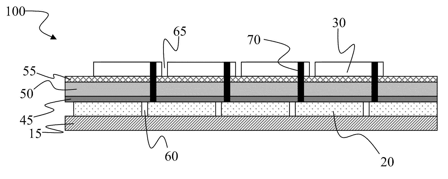
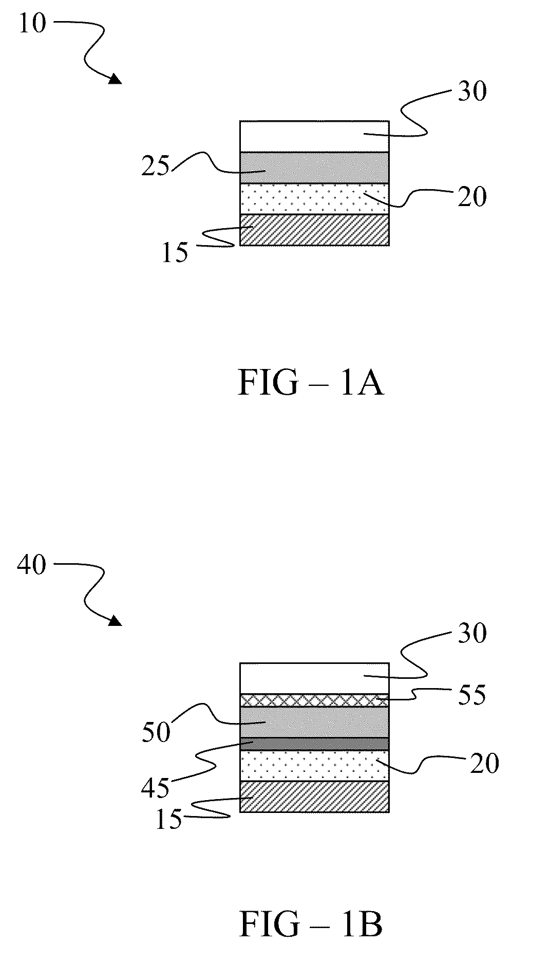
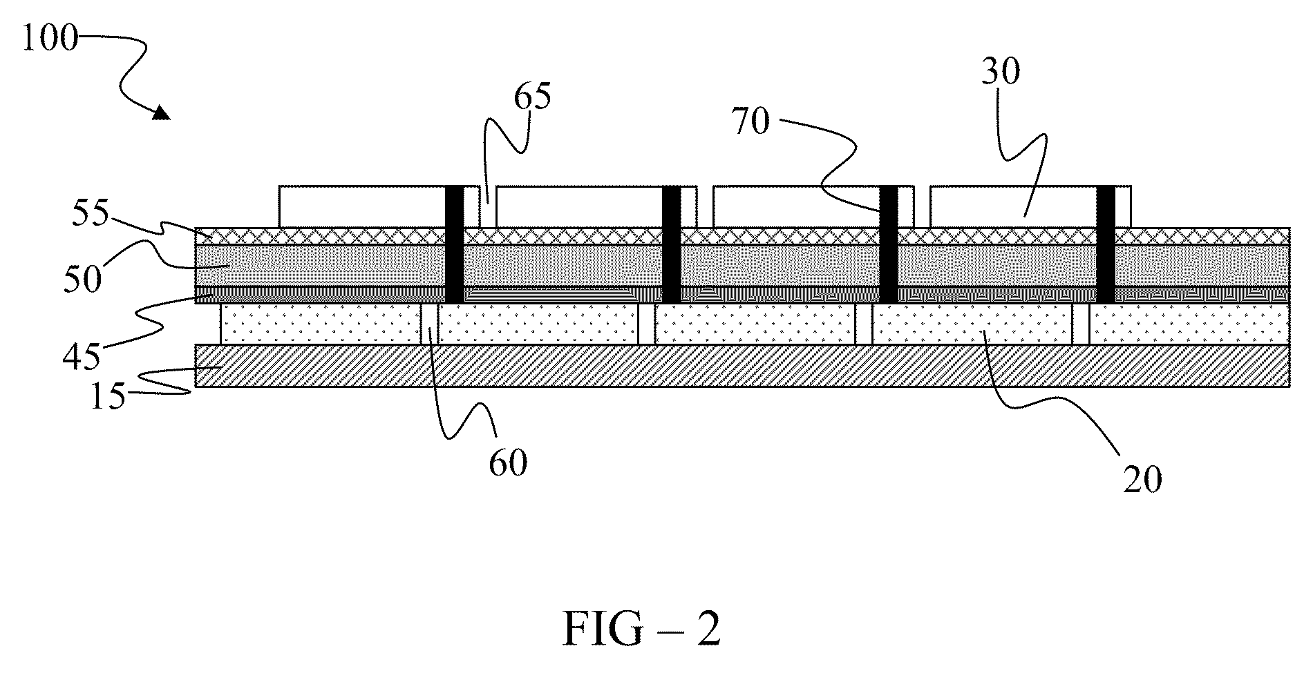
[0036]As used herein, “on” signifies direct contact of a particular layer with another layer and “over” signifies that a particular layer is mechanically supported by another layer. If a particular layer, for example, is said to be formed on a substrate, the layer directly contacts the substrate. If a particular layer is said to be formed over a substrate, the layer is mechanically supported by the substrate and may or may not make direct contact with the substrate. If a particular layer is said to be formed ...


PUM

PropertyMeasurementUnit
temperatureaaaaaaaaaa

Abstract

A photovoltaic device and method of forming a photovoltaic device. The photovoltaic device includes a fluorine-containing photovoltaic material and a transparent electrode. Inclusion of fluorine in the photovoltaic material increases its thermal stability. The effect is particularly pronounced in photovoltaic materials based on disordered forms of silicon, including amorphous, nanocrystalline, or microcrystalline silicon. The higher thermal stability permits deposition or annealing of the transparent electrode at high temperature. As a result, high conductivity is achieved for the transparent electrode without degrading the photovoltaic material. The higher conductivity of the transparent electrode facilitates series integration of individual devices to form a module. The method includes forming a photovoltaic material from a fluorinated precursor or treating a photovoltaic material in a fluorine-containing ambient.

Description

FIELD OF INVENTION[0001]This invention relates to the high speed manufacturing of photovoltaic devices. More particularly, this invention relates to formation and integration of solar cells from photovoltaic materials in a continuous manufacturing process. Most particularly, this invention relates to the continuous deposition of silicon-based photovoltaic cells formed by a process that includes a high temperature step for forming a transparent conducting electrode.BACKGROUND OF THE INVENTION[0002]Concern over the depletion and environmental impact of fossil fuels has stimulated strong interest in the development of alternative energy sources. Significant investments in areas such as batteries, fuel cells, hydrogen production and storage, biomass, wind power, algae, and solar energy have been made as society seeks to develop new ways of creating and storing energy in an economically competitive and environmentally benign fashion. The ultimate objective is to minimize society's relian...

Claims


Application Information

Patent Timeline
Patent Type & Authority Applications(United States)
IPC IPC(8): H01L31/05H01L31/0232H01L31/18
CPCH01L31/022466H01L31/035218H01L31/03685H01L31/03762H01L31/1884H01L31/056Y02E10/52Y02E10/545Y02E10/548H01L31/046H01L31/202Y02P70/50
Inventor OVSHINSKY, STANFORD R.
Owner OVSHINSKY TECH
Why Eureka
Try Eureka