

Semiconductor device and method of manufacturing a semiconductor device
a semiconductor and semiconductor technology, applied in the direction of semiconductor devices, electrical appliances, basic electric elements, etc., can solve the problems of uneven application of resists, increase in gap between semiconductor substrates and insulating films, and decrease in device breakdown voltage, so as to prevent the generation of uneven applications and improve the focus margin
- Summary
- Abstract
- Description
- Claims
- Application Information
AI Technical Summary
Benefits of technology
Problems solved by technology
Method used
Image

Examples
first preferred embodiment
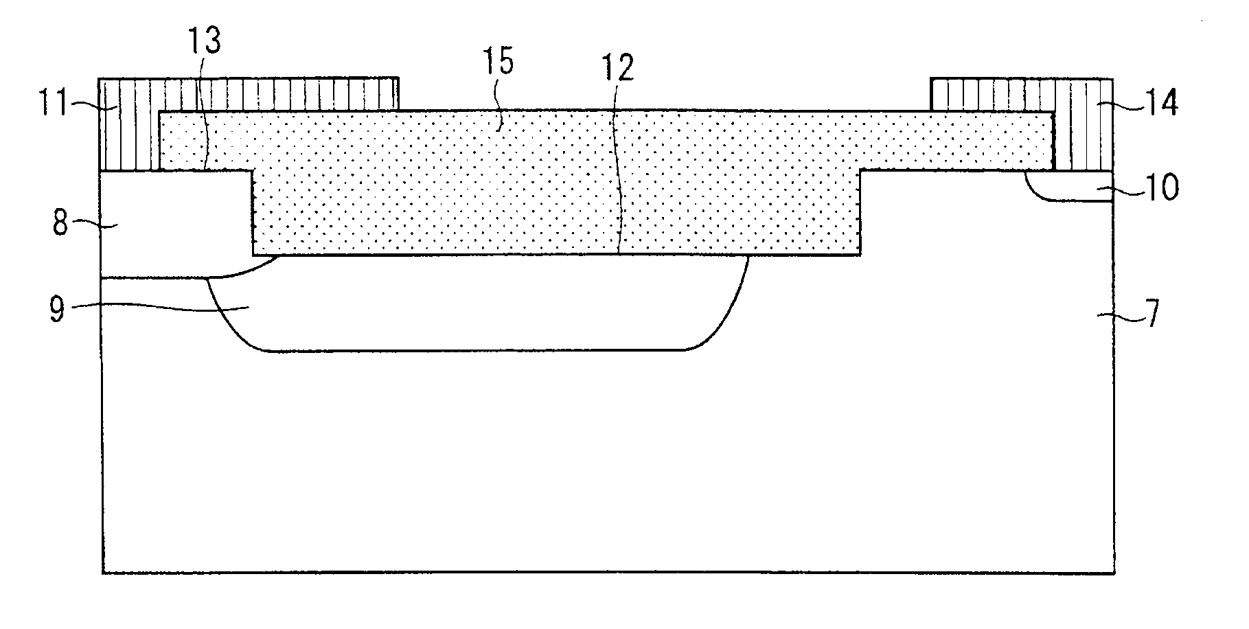
[0034]FIG. 1 is a cross-sectional view showing a structure of a junction termination end of a high-breakdown-voltage semiconductor device (diode) according to a first preferred embodiment.
[0035]In the structure shown in FIG. 1, an electrode layer 8 of p type conductivity is formed in a surface of a semiconductor substrate 7 of n type conductivity. On an upper surface of the semiconductor substrate 7, a recessed part 12 is formed. The recessed part 12 is formed so as to intersect the electrode layer 8, and a part of the recessed part 12 is formed in the electrode layer 8. That is, the electrode layer 8 and the recessed part 12 are adjacent to each other. In the structure shown in FIG. 1, the bottom surface of the electrode layer 8 is located at a position deeper than the recessed part 12.
[0036]A reduced surface field (RESURF) layer 9 is formed in the semiconductor substrate 7 so as to surround the electrode layer 8. The RESURF layer 9 is composed of p type (p-type) impurities having ...
second preferred embodiment
[0061]FIG. 10 shows simulation results, which shows the correlation between the depth of the RESURF layer 9 and the breakdown voltage of the high-breakdown-voltage semiconductor device (600 V class).
[0062]As can be seen from FIG. 10, the depth of the RESURF layer 9 is increased, whereby the breakdown voltage of the semiconductor device is improved. However, the impurity concentration of the RESURF layer 9 is approximately 1.0E15 atoms / cm3, which is extremely small. Accordingly, in order to form a deep RESURF layer 9, the thermal diffusion treatment for an extremely long period of time is required.
[0063]FIG. 11 shows simulation results, which shows the relationship between a drive time (thermal diffusion treatment time) and a depth of a diffusion layer in a case where the thermal diffusion treatment at 1,200° C. is assumed. In this simulation, the case is assumed where boron is implanted into an n type silicon substrate having a specific resistance of 23 Ω·cm on the conditions of acc...
third preferred embodiment
[0083]The description above has been given of a fact that a gap between the upper surface 13 of the semiconductor substrate 7 and the upper surface of the insulating film 15 is increased, whereby unevenness occurs in resist application when a resist is applied onto the gap. FIG. 18 shows experimental results, which shows the generation of unevenness in resist application that results from the gap. The experimental results shown in FIG. 18 are obtained by forming multiple types of gaps and the presence / absence of the generation of unevenness in resist application was examined for each gap.
[0084]In the experiment in which the results of FIG. 18 were obtained, oxidize films having different thicknesses were formed on an eight-inch silicon wafer, and the multiple types of gaps (five types of gaps: 0.5 μm, 0.8 μm, 1.0 μm, 1.5 μm and 2.0 μm) described above were formed. Then, a positive resist having viscosity of 19 cp was applied onto the gaps at the number of revolutions of 1,400 rpm, t...
PUM
 Abstract
Description
Claims
Application Information