method of manufacturing a gas electron multiplier

Inactive Publication Date: 2011-04-21
EUROPEAN ORGANIZATION FOR NUCLEAR RESEARCH
View PDF5 Cites 16 Cited by
  • Summary
  • Abstract
  • Description
  • Claims
  • Application Information

AI Technical Summary

Benefits of technology

[0017]Preferably, the electrochemical etching of the second metal layer from the inside, i.e. through the holes formed in the first metal layer and the insulating sheet, is maintained until said holes are extended into the second metal layer to an average depth that is at least 2 μm deeper than the final thickness of the second metal layer. Then, when the second metal layer is etched from the outside, the holes in the second metal layer will be uncovered, and the edges of the holes will have a consistent quality.
[0018]In a preferred embodiment, the initial thickness of the second metal layer exceeds the initial thickness of the first metal layer by 5

Problems solved by technology

When trying to manufacture bigger GEMs, the inventor found that difficulties arise with the prior art manufacturing method.
In particular, for larger GEMs it turns out to be very difficult to ensure a proper co-registering of the patterns on both sides of the blank.
While it is possible to print these masks with sufficient precision, it turned out that the film on which the masks were printed were not stable enough to guarantee a precise alignment of the pattern on both sides of the blank if the films are becoming larger such as to form a larg

Method used


Image

  •  method of manufacturing a gas electron multiplier
  •  method of manufacturing a gas electron multiplier
  •  method of manufacturing a gas electron multiplier

Examples


Example

Second Embodiment

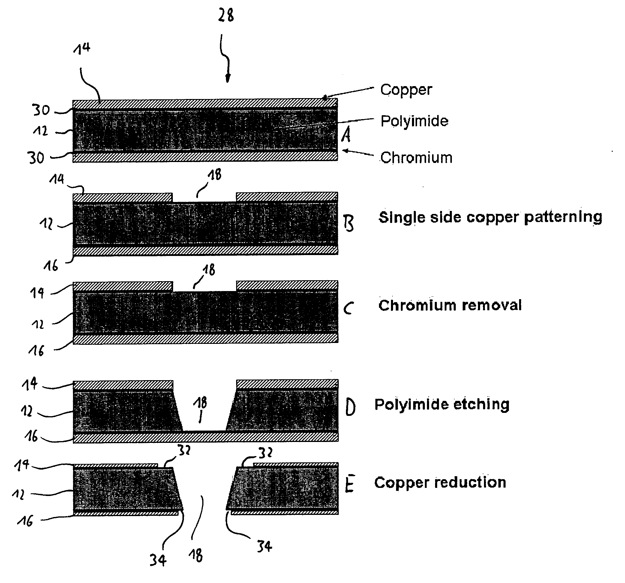
[0052]Next, a second embodiment of the invention is described with reference to FIG. 5. As is seen in panel A of FIG. 5, again a blank sheet 28 is prepared having a polyimide insulating layer 12 and first and second copper layers 14, 16 on top of its first and second surfaces. However, in this case, the blank 28 is prepared such that the second copper layer 16 is thicker than the first copper layer 14. In the example shown, the first copper layer 14 is 5 μm thick and the second copper layer 16 is 15 μm thick. Such a blank 28 can be prepared by electrolytically adding 10 μm of copper to the second metal layer 16 of an original blank (not shown) having 5 μm of copper cladding on each side.

[0053]The patterning of the first copper layer 14 and the underlying chromium layer is performed similarly as described in section 1.1. above and shall not be repeated here. Panel B of FIG. 5 shows the blank sheet 28 after patterning, where in contrast to FIG. 4, the formation of fou...

Example

[0054]The insulating sheet hole forming step is also similar to that of the first embodiment described in section 1.2. above. However, as compared to panel D of FIG. 4, the holes 18 formed in the polyimide layer 12 in this instance are more cylindrical. This is achieved by stirring the etchant by means of nitrogen bubbles. The first and second side ends of the hole 18 through the polyimide layer 12 differs by less than 5 μm. It is to be understood that more cylindrical holes could be used in the first embodiment and more conical holes could be used in the second embodiment as well. Also, the steps of forming the electrodes 24, 26 (see FIG. 2) and the frame 22 surrounding the active area 20 are performed in a way similar to the first embodiment.

[0055]The main difference with regard to the first embodiment relates to the second metal layer hole forming step. For forming the holes through the second copper layer 16, in this embodiment, the blank sheet 28 is immersed in a bath based on ...


PUM

PropertyMeasurementUnit
Temperatureaaaaaaaaaa

Abstract

Methods for manufacturing a gas electron multiplier. One method comprises a step of preparing a blank sheet comprised of an insulating sheet with first and second metal layers on its surface, a first metal layer hole forming step in which the first metal layer is patterned by means of photolithography, such as to form holes through the first metal layer, an insulating sheet hole forming step, in which the holes formed in the first metal layer are extended through the insulating layer by etching from the first surface side only, and a second metal layer hole forming step, in which the holes are extended through the second metal layer. Alternatively, the second metal layer hole forming step is performed by electrochemical etching, such that the first metal layer remains unaffected during etching of the second metal layer. In another embodiment, in the second metal layer hole forming step, the first and second metal layers are etched from the outside, thereby reducing the initial thicknesses of the first and second metal layers and the second metal layer is simultaneously etched through the holes in the first metal layer and the insulating sheet, said etching being maintained until the holes extend through the second metal layer, wherein said initial average thickness of the first and second metal layers is between 6.5 μm and 25 μm, preferably between 7.5 μm and 12 μm.

Description

[0001]The present application is a US national stage application filed, under 35 U.S.C. §371, on the basis of International Application PCT / EP2008 / 0002944, filed Apr. 14, 2008, which is incorporated herein by reference.BACKGROUND OF THE INVENTION[0002]The present invention relates to a method for manufacturing a gas electron multiplier (GEM). The structure and the operation of a GEM are described in EP 0 948 803 B1, in which also a number of further references are given. FIG. 1 is a schematic diagram taken from EP 0 948 803 B1 showing the general structure and function of a GEM. In FIG. 1, a GEM 10 is located between a drift electrode DE and a collecting electrode CE. The GEM 10 consists of an insulator sheet 12 which is cladded with first and second metal layers 14, 16. In the GEM 10, a plurality of throughholes 18 are formed. The throughholes 18 typically have a diameter of 20 to 100 μm. The holes 18 are arranged in a matrix or array pattern with a pitch of typically 50 to 300 μm....

Claims


Application Information

Patent Timeline
IPC IPC(8): H01J43/06C23F1/00C25F3/02C25D5/48
CPCH01J47/02
Inventor DE OLIVEIRA, RUIDUARTE PINTO, SERGE
Owner EUROPEAN ORGANIZATION FOR NUCLEAR RESEARCH
Why Eureka
Try Eureka