Mos transistor resistor, filter, and integrated circuit

Inactive Publication Date: 2011-04-28
PANASONIC CORP
View PDF13 Cites 5 Cited by
  • Summary
  • Abstract
  • Description
  • Claims
  • Application Information

AI Technical Summary

Benefits of technology

[0028]According to the present invention, the gate voltage Vg and the input voltage Vin are set in an appropriate manner to satisfy the conditions under which the first MOS transistor operates in the non-saturation region and the t

Problems solved by technology

With this, it is difficult to achieve a normal function as a filter.
Accordingly the effect of temperature characteristic

Method used


Image

  • Mos transistor resistor, filter, and integrated circuit
  • Mos transistor resistor, filter, and integrated circuit
  • Mos transistor resistor, filter, and integrated circuit

Examples


embodiment 1

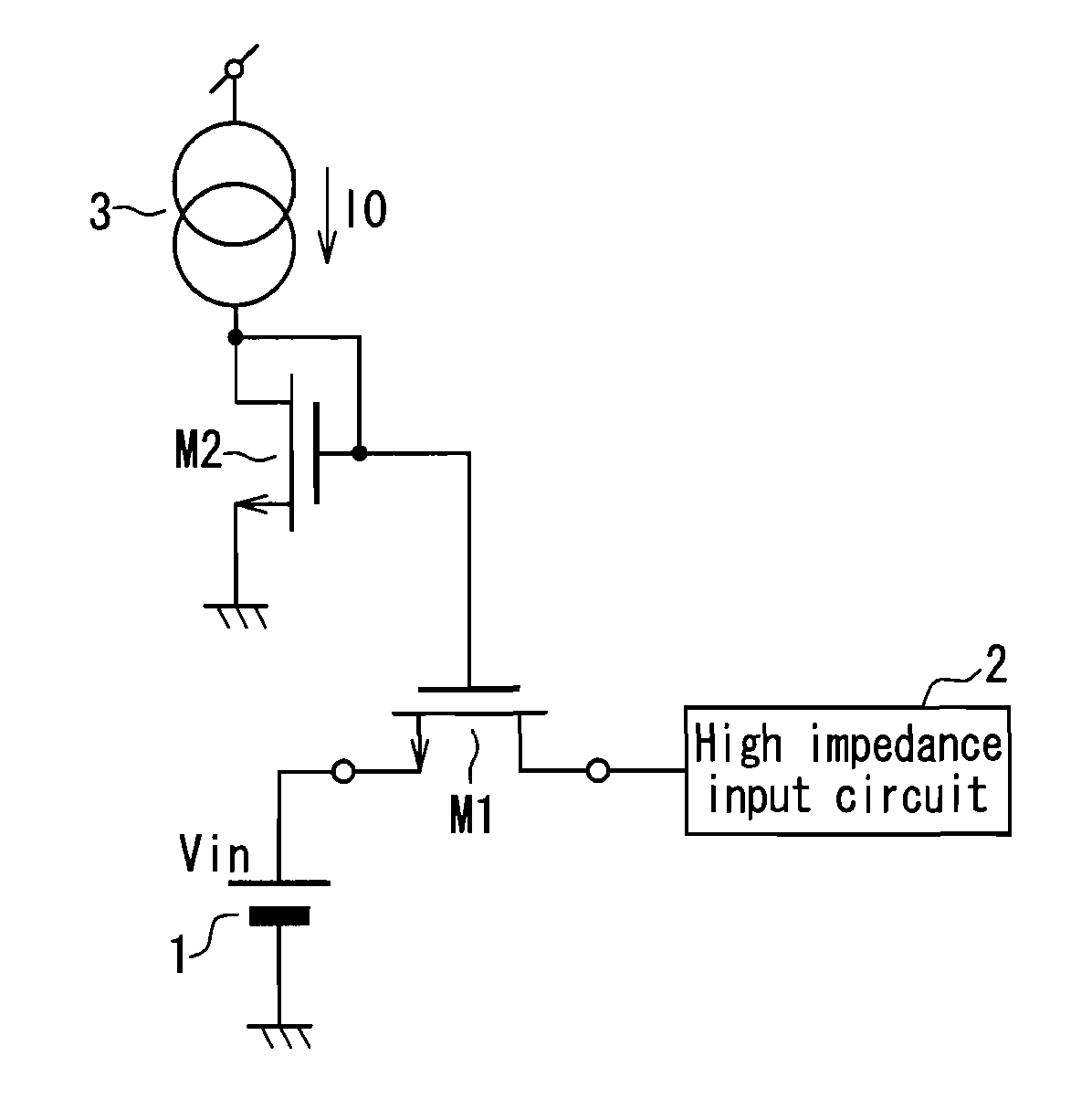
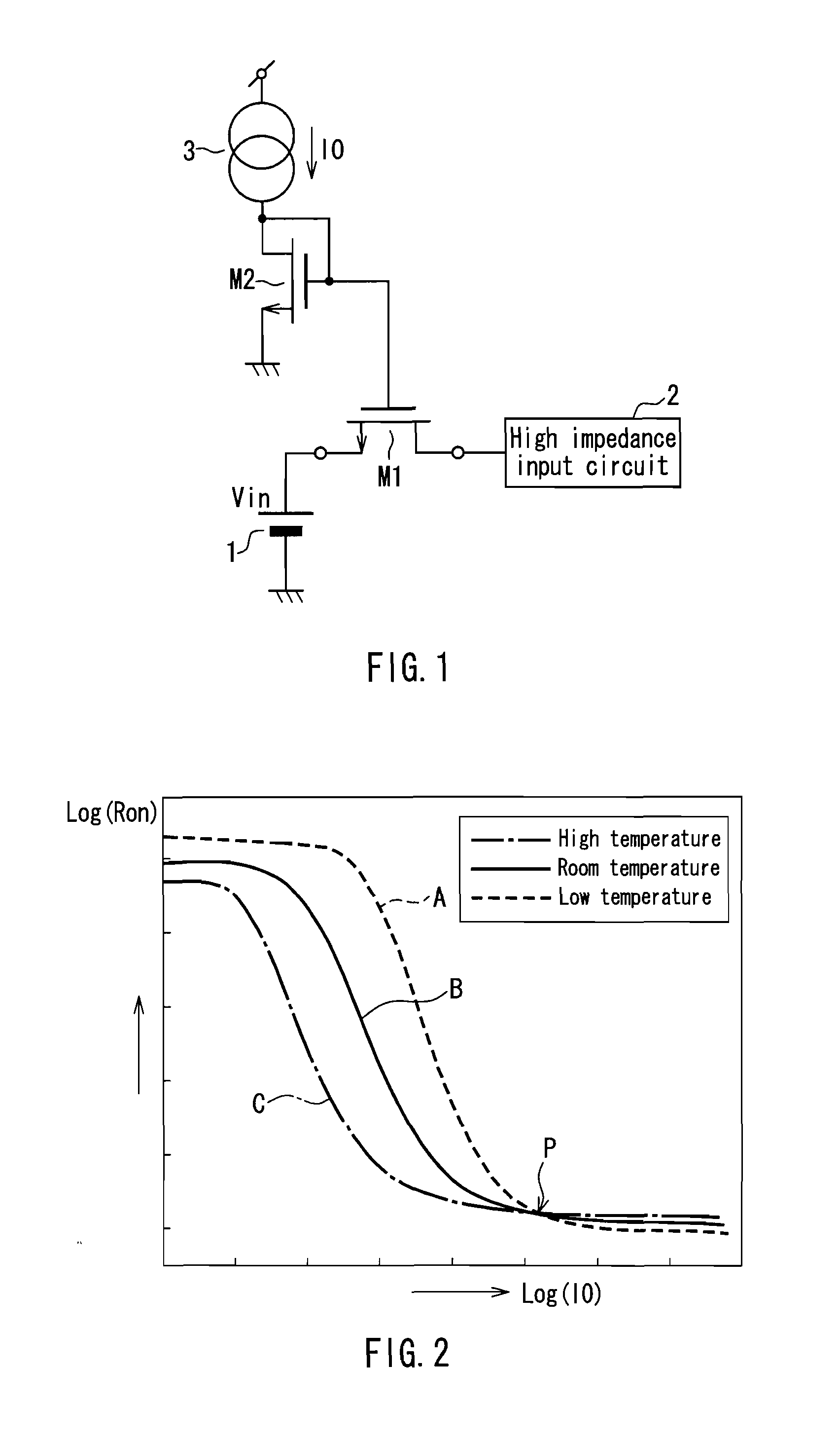
[0049]FIG. 1 is a circuit diagram showing a MOS transistor resistor according to Embodiment 1. This MOS transistor resistor is composed of MOS transistors M1, M2 and an input voltage source 1 (voltage Vin). As for the MOS transistor M1, its source is grounded through the input voltage source 1 and its drain is connected to a high impedance input (high input resistance) circuit 2 as a following stage circuit. To the gate of the MOS transistor M1, voltages generated by the MOS transistor M2 and the current source 3 (current I0) are applied.

[0050]The operation of the MOS transistor resistor configured as above will be described. Also for this MOS transistor resistor, the resistance value is expressed by the Formula 4. In the following description, the same symbols are used for elements that are similar to the formula elements that have been used to describe the prior art and are described with numerals related to the reference numerals of the MOS transistors corresponding thereto.

Ron=L...

embodiment 2

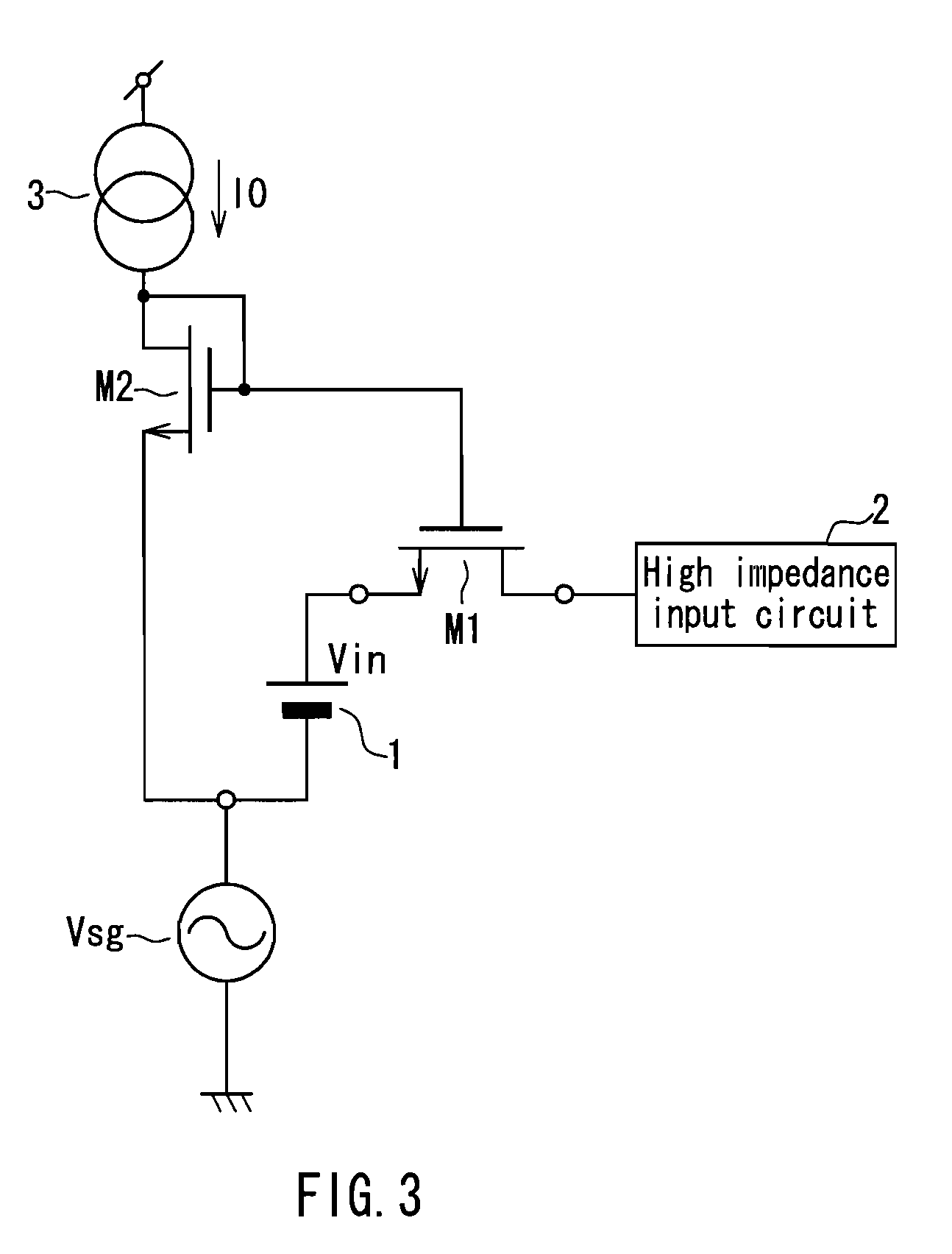
[0068]FIG. 10 is a circuit diagram showing a MOS transistor resistor according to Embodiment 2 of the present invention. This MOS transistor resistor is different from the configuration of the MOS transistor resistor according to Embodiment 1 shown in FIG. 1 in that the MOS transistor M2 is replaced with a gate voltage source 6 (voltage Vg). That is, a voltage Vg of the gate voltage source 6 is applied to the gate of the MOS transistor M1.

[0069]In the configuration of FIG. 10. by setting the voltage Vg to the same voltage as the gate-source voltage VGS2 of the MOS transistor M2 of FIG. 1, the exact same effects as those achieved by the MOS transistor resistor according to Embodiment 1 can be achieved. That is, by setting the gate voltage Vg to the gate-source voltage VGS2 that is expressed by Formula 16, in other words, to a voltage obtained by adding to the threshold voltage VTH the input voltage Vin×2, the temperature characteristics of the resistance value Ron can be canceled.

[00...


PUM


Abstract

A MOS transistor including a first MOS transistor M1 to be used as a resistor; an input voltage source 1 connected to the source of the first MOS transistor for applying an input voltage Vin; and a gate voltage source 6 connected to the gate of the first MOS transistor for applying a gate voltage Vg. The gate voltage Vg and the input voltage Vin are set within a range where a gate-source voltage and source-drain voltage of the first MOS transistor cause the first MOS transistor to operate in a non-saturation region and also are set to avoid the first MOS transistor operating in an operation region with leakage current. Fluctuations of the resistance value resulting from a change in leakage current due to manufacturing variations are reduced and favorable temperature characteristics are obtained.

Description

BACKGROUND OF INVENTION[0001]1. Field of the Invention[0002]The present invention relates to resistors utilizing MOS transistors, and particularly to a MOS transistor resistor suited for electronic devices that perform voice signal processing of a microphone, to signal processing of a sensor and to integrated circuits of the electronic devices.[0003]2. Description of Related Art[0004]Conventionally, it has been known to use MOS transistors as resistors. As an example of use of a MOS transistor resistor of such a type, FIG. 11 shows a voltage comparison circuit disclosed in JP S57-108670 A (page 3, FIG. 2).[0005]The voltage comparison circuit is composed of a comparator 7, MOS transistors M5, M6 and a capacitor C. An input signal from a signal source Vsg is inputted through the capacitor C, and the MOS transistors M5, M6 are used as a resistor.[0006]The operation of the resistor composed of the MOS transistors M5, M6 in the voltage comparison circuit will be described hereinafter. Wh...

Claims


Application Information

Patent Timeline
IPC IPC(8): H03H11/24
CPCH01L27/0802H03H11/245H01L27/088H03H11/53H03H11/04
Inventor OZASA, MASAYUKIMASAI, SHIGEOKOBAYASHI, HITOSHIYAMASAKI, SHUYA
Owner PANASONIC CORP
Why Eureka
Try Eureka