Layer for thin film photovoltaics and a solar cell made therefrom

a solar cell and thin film technology, applied in the field of photovoltaics, can solve the problems of low efficiency of solar cell manufacturing, and high cost of conventional solar cells, and achieve the effect of high carrier density

Inactive Publication Date: 2011-05-05
FIRST SOLAR INC (US)
View PDF10 Cites 11 Cited by
  • Summary
  • Abstract
  • Description
  • Claims
  • Application Information

AI Technical Summary

Benefits of technology

[0009]Still yet another embodiment is a method. The method comprises a first step of providing an absorber layer in a photovoltaic device. The absorber layer is treated to increase its carrier density. Further, the absorber layer is etched to provide a stoichiometric absorber layer. The absorber layer comprises a p-type semiconductor. The absorber layer is substantially free of silicon. At least one layer is disposed over the absorber layer. The at least one layer is a semiconductor having a higher carrier density than the carrier density of the absorber layer. The at least one layer comprises a p+-type semiconductor. The at least one layer comprises silicon.

Problems solved by technology

Unfortunately, the available solar energy is not generally used efficiently to produce electricity.
The cost of conventional solar cells, and electricity generated by these cells, is generally very high.
Moreover, solar cells typically include multiple layers formed on a substrate, and thus solar cell manufacturing typically requires a significant number of processing steps.
As a result, the high number of processing steps, layers, interfaces, and complexity increase the amount of time and money required to manufacture these solar cells.

Method used


Image

  • Layer for thin film photovoltaics and a solar cell made therefrom
  • Layer for thin film photovoltaics and a solar cell made therefrom
  • Layer for thin film photovoltaics and a solar cell made therefrom

Examples


Embodiment Construction

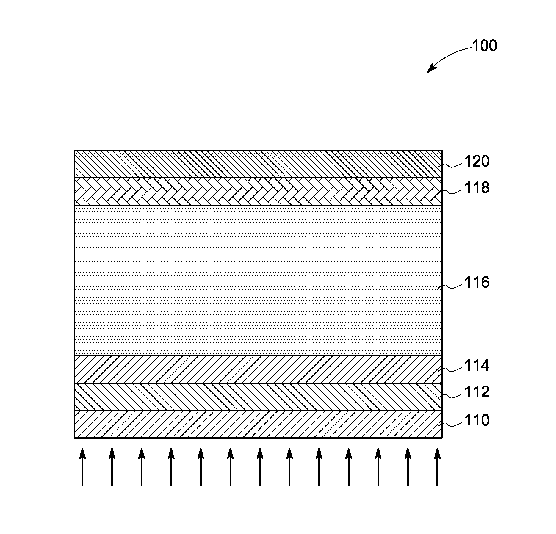
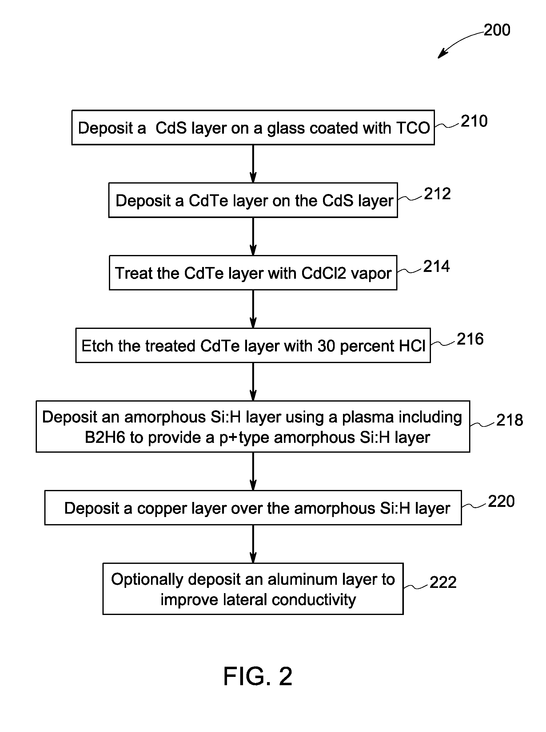
[0014]Cadmium telluride (CdTe) based solar devices known in the art typically demonstrate relatively low power conversion efficiencies, which may be attributed to a relatively low open circuit voltage (Voc) in relation to the band gap of the material. Further issues with improving the cell efficiency of CdTe solar cells include the high work function of CdTe. The high work function of CdTe leaves a narrow choice of metals that can be employed to form an Ohmic contact with the CdTe layer. The metals include platinum and gold, which are not commercially viable metals for low-cost mass-production of the CdTe solar cells. However, though other metals like molybdenum, nickel, chromium, etc. may be employed, they form a barrier; for example, in the case of p-type CdTe, the holes will need to tunnel through the barrier region. As CdTe has typical carrier densities between 1×10¹⁴ and 1×10¹⁵ per cubic centimeter, this barrier may be relatively large. It has been found that without proper tre...


PUM


Abstract

A photovoltaic device is provided. The photovoltaic device comprises an absorber layer comprising a p-type semiconductor, wherein at least one layer is disposed over the absorber layer. The at least one layer is a semiconductor having a higher carrier density than the carrier density of the absorber layer. The at least one layer comprises silicon. The at least one layer comprises a p+-type semiconductor. The absorber layer is substantially free of silicon. A method of forming the photovoltaic device is provided.

Description

BACKGROUND[0001]The invention relates generally to the field of photovoltaics. In particular, the invention relates to a layer used in a photovoltaic device and a solar panel made therefrom.[0002]Solar energy is abundant in many parts of the world year around. Unfortunately, the available solar energy is not generally used efficiently to produce electricity. The cost of conventional solar cells, and electricity generated by these cells, is generally very high. For example, a typical solar cell achieves a conversion efficiency of less than 20 percent. Moreover, solar cells typically include multiple layers formed on a substrate, and thus solar cell manufacturing typically requires a significant number of processing steps. As a result, the high number of processing steps, layers, interfaces, and complexity increase the amount of time and money required to manufacture these solar cells.[0003]Accordingly, there remains a need for an improved solution to the long-standing problem of inef...

Claims


Application Information

Patent Timeline
Patent Type & Authority Applications(United States)
IPC IPC(8): H01L31/18H01L31/00
CPCH01L31/0296Y02E10/50H01L31/1836
Inventor KOREVAAR, BASTIAAN ARIEXI, YANGANG ANDREWAHMAD, FAISAL RAZIJOHNSON, JAMES NEIL
Owner FIRST SOLAR INC (US)
Why Eureka
Try Eureka