UV and reducing treatment for k recovery and surface clean in semiconductor processing

a technology of reducing treatment and semiconductor processing, applied in the direction of cleaning process and apparatus, cleaning process using liquids, chemistry apparatus and processes, etc., can solve the problems of inherently weak low-k dielectric material, affecting and affecting downstream electronic-packaging process and material compatibility, etc., to achieve effective post-planarization surface cleaning and improve the adhesion of subsequently applied dielectric barriers

Active Publication Date: 2011-05-12
NOVELLUS SYSTEMS
View PDF100 Cites 71 Cited by
  • Summary
  • Abstract
  • Description
  • Claims
  • Application Information

AI Technical Summary

Benefits of technology

[0009]The present invention provides a method for treatment of carbon-containing low-k dielectric, for example, but not limited to carbon-doped oxide (CDO), and possibly including a metal feature, with a reducing agent and ultraviolet (UV) radiation, for the repair of process-induced damage. In another aspect, treatment with a reducing agent and ultraviolet (UV) radiation is effective to clean a processed wafer surface by removal (reduction) of metal oxide (e.g.,

Problems solved by technology

These low-k dielectrics are mechanically weaker than previous generation dielectric materials.
The inherently weak nature of the low-k dielectric material can pose significant challenges for downstream electronic-packaging processes and material compatibility.
This low density introduces a host of process integration and material compatibility difficulties.
Achieving a balance between maintaining a low-k film's integrity, integrating it properly, and performing the necessary stripping, cleaning, and conditioning is challenging.
The properties that give carbon-containing low-k dielectric materials their desirable low dielectric constants are the very same properties that are leading to significant integration challenges.
Because of the mechanical weakness, carbon-containing low-k films are susceptible to kinetic plasma damage that can undesirably densify the film and thus increase the film's effective k value.
The susceptibility of carbon-containing low-k materials to plasma modification poses a

Method used


Image

  • UV and reducing treatment for k recovery and surface clean in semiconductor processing
  • UV and reducing treatment for k recovery and surface clean in semiconductor processing
  • UV and reducing treatment for k recovery and surface clean in semiconductor processing

Examples


examples

[0070]The following provides examples of specific implementations of the present invention and performance data in order to give a better understanding of the invention. The invention is, however, in no way limited to these specific implementations.

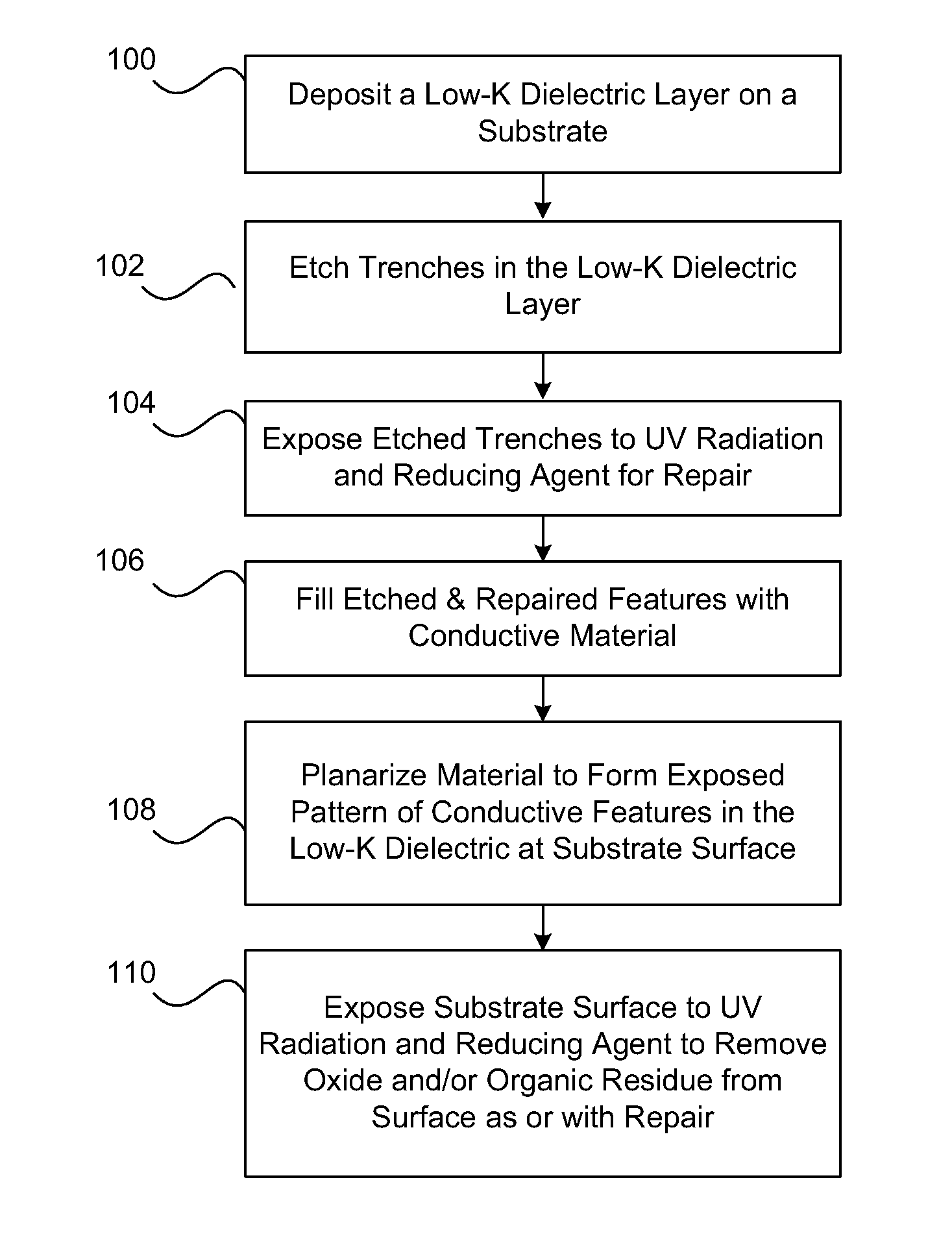
[0071]Post-CMP Processing

[0072]In one embodiment of the invention, NH3 was used as the reducing agent. NH3 absorbs in the UV range, and can potentially create H radicals which can reduce metal oxide. Both the H radicals and exposure to UV radiation can potentially remove the residual CMP organic residue (C removal). In this example, very high curing pressures (about 600T) were used in order to increase generation of H radicals, but lower pressures can also be potentially used, depending on the amount of metal oxide that needs to be removed.

[0073]In order to evaluate metal oxide (CuOx in this case) removal, about 130 Å of CuO was grown using an oxidizing plasma on PVD Cu. The impact of different cure times, and impact with and without UV e...


PUM


Abstract

Treatment of carbon-containing low-k dielectric with UV radiation and a reducing agent enables process-induced damage repair. Also, treatment with a reducing agent and UV radiation is effective to clean a processed wafer surface by removal of metal oxide (e.g., copper oxide) and/or organic residue of CMP slurry from the planarized surface of a processed wafer with or without low-k dielectric. The methods of the invention are particularly applicable in the context of damascene processing to recover lost low-k property of a dielectric damaged during processing, either pre-metalization, post-planarization, or both, and/or provide effective post-planarization surface cleaning to improve adhesion of subsequently applied dielectric barrier and/or other layers.

Description

CROSS-REFERENCE TO RELATED APPLICATION[0001]This application claims priority to U.S. Provisional Patent Application No. 61 / 260,789 filed Nov. 12, 2009, titled UV AND REDUCING TREATMENT FOR K RECOVERY AND SURFACE CLEAN IN SEMICONDUCTOR PROCESSING. This provisional patent application is incorporated herein by reference in its entirety for all purposes.BACKGROUND OF THE INVENTION[0002]The invention relates to semiconductor processing, in particular to surface cleaning and repair of process-induced damage of low dielectric constant dielectric materials in, for example, damascene processing.[0003]Low dielectric constant (low-k) insulating materials have been integrated into semiconductor devices in order to address reduced feature sizes and high performance requirements. These low-k dielectrics are mechanically weaker than previous generation dielectric materials. The inherently weak nature of the low-k dielectric material can pose significant challenges for downstream electronic-packagi...

Claims


Application Information

Patent Timeline
IPC IPC(8): H01L21/02B08B3/00
CPCH01L21/02063H01L21/02074H01L21/3105H01L21/67115H01L21/76883H01L21/76825H01L21/76826H01L21/76831H01L21/76877H01L21/76814
Inventor VARADARAJAN, BHADRIANTONELLI, GEORGE A.VAN SCHRAVENDIJK, BART
Owner NOVELLUS SYSTEMS
Why Eureka
Try Eureka