

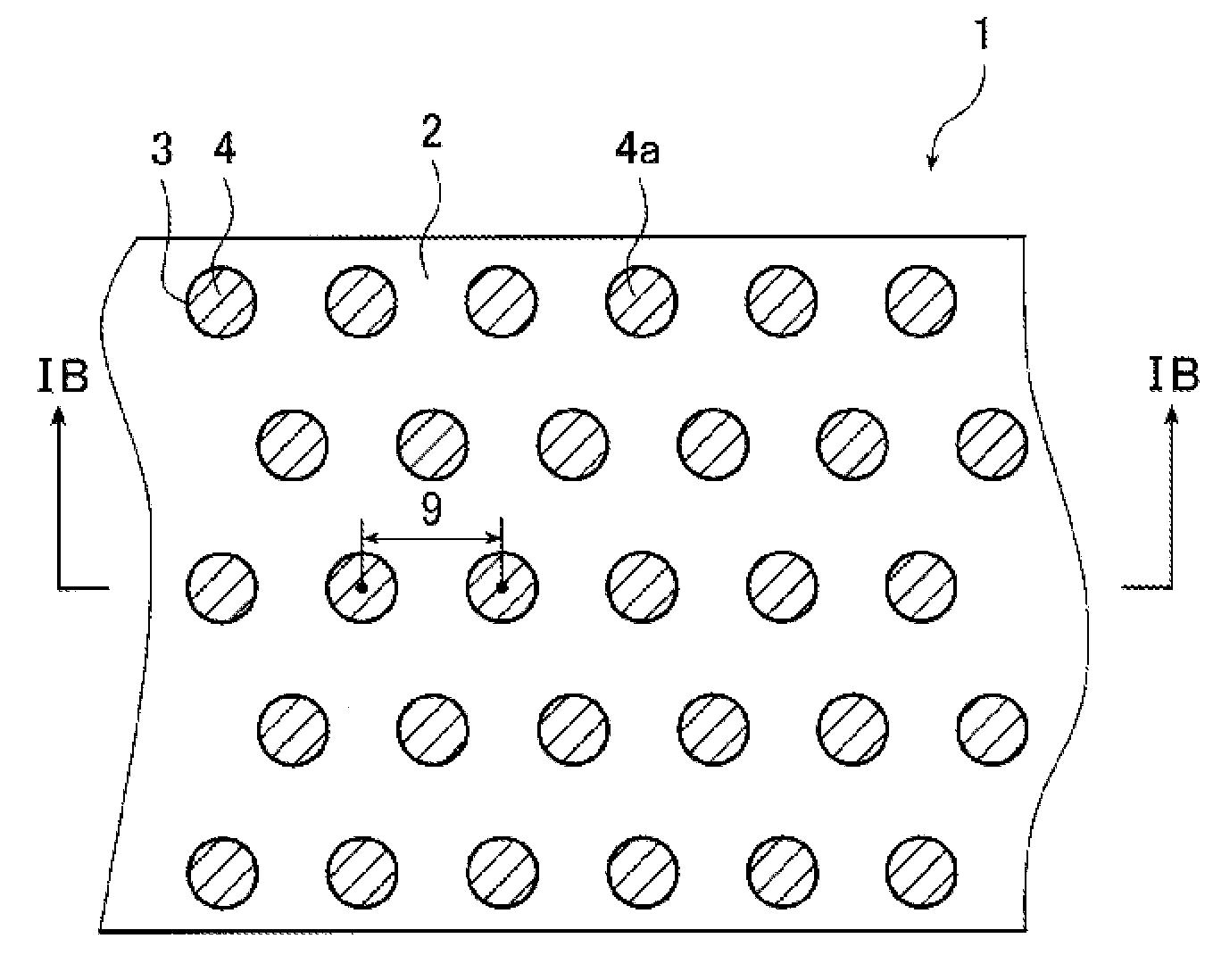
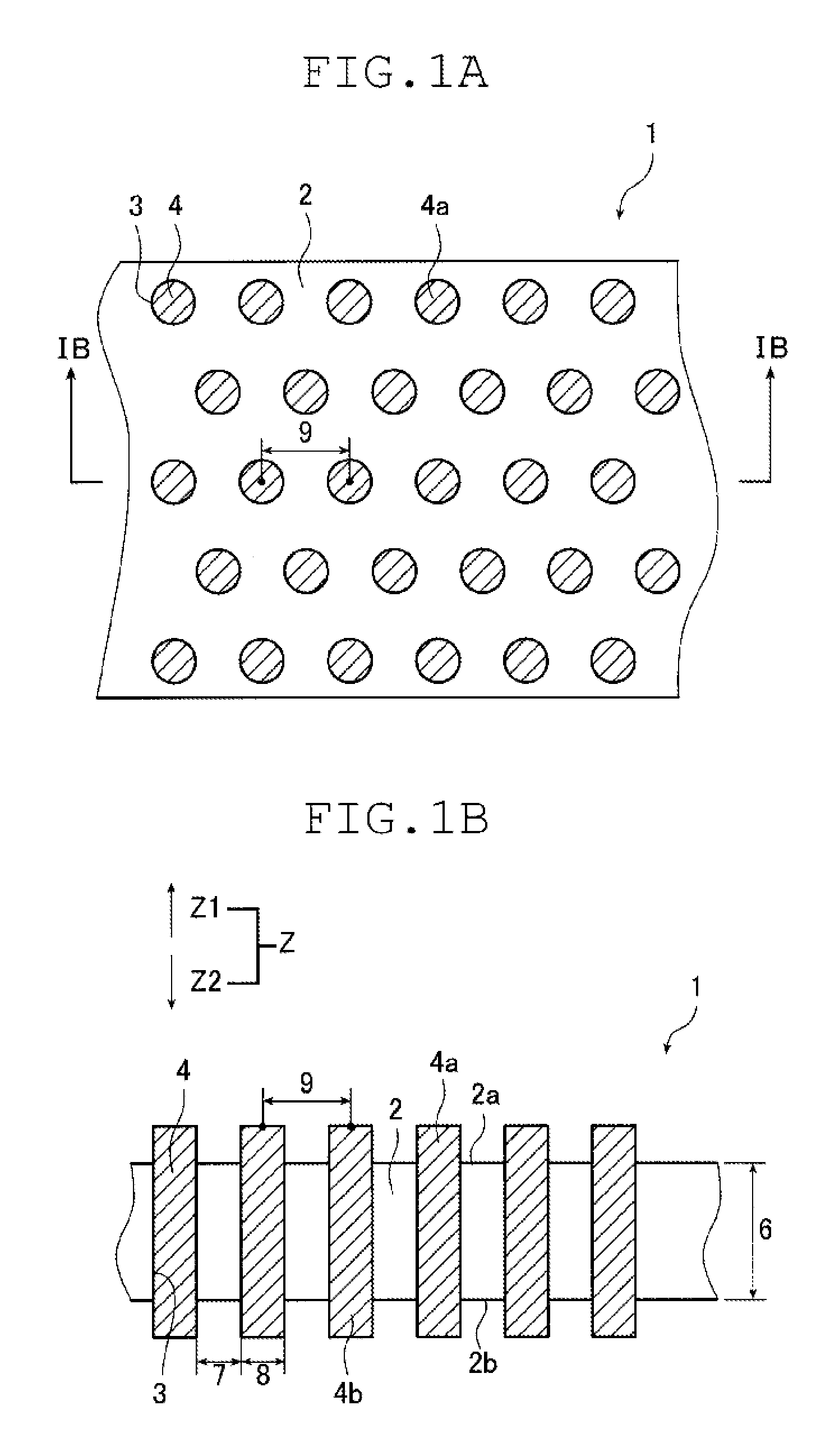
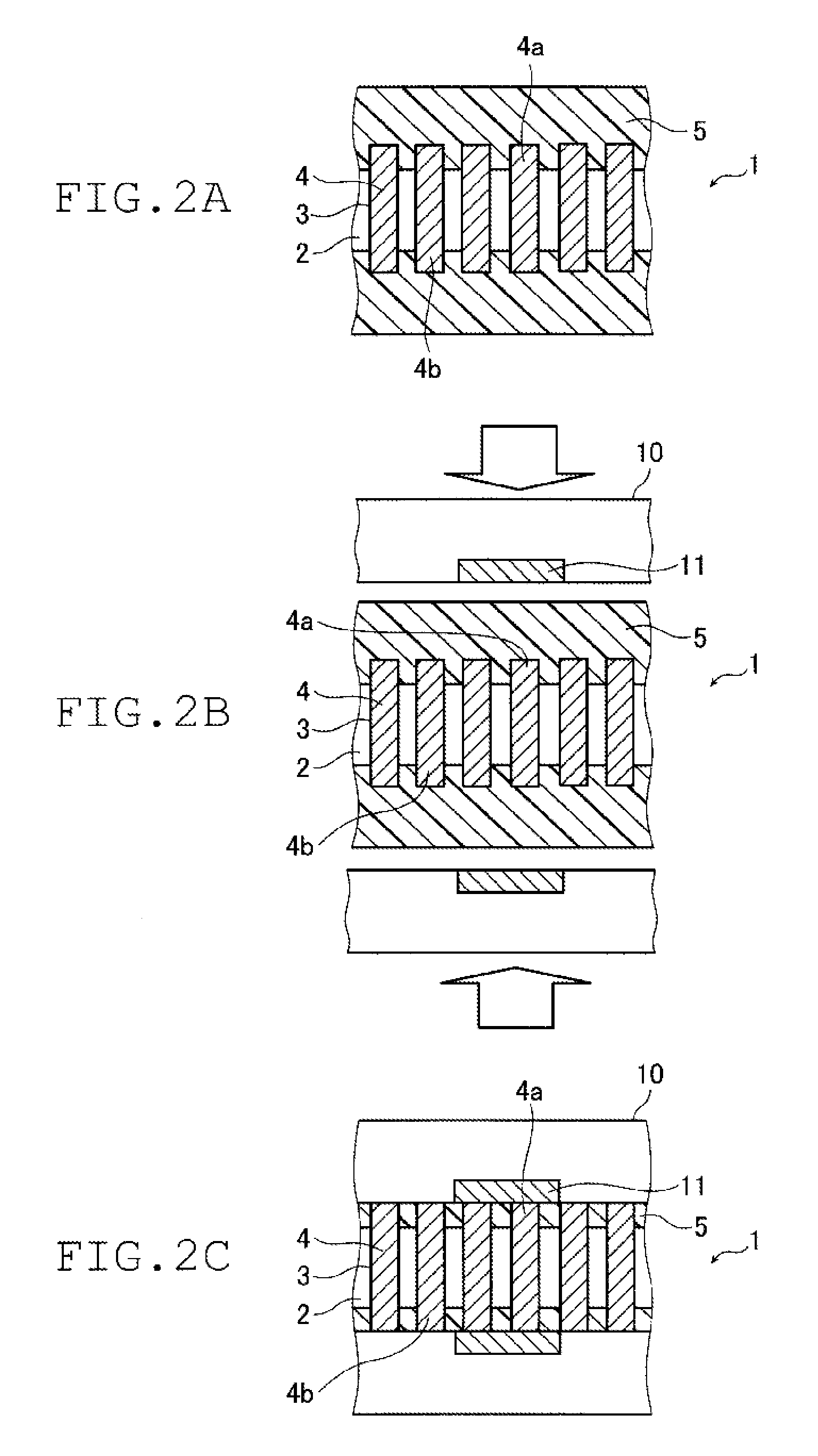
Microstructure, and method for production thereof
a microstructure and microstructure technology, applied in the field of microstructure, can solve the problems of difficult to reduce the size of the conductive path, difficult to fill the conductive material at a high filling ratio, and the inability to fully guarantee the connection stability of conventional techniques, etc., to achieve excellent long-term stability, simple joining, and high joint strength
- Summary
- Abstract
- Description
- Claims
- Application Information
AI Technical Summary
Benefits of technology
Problems solved by technology
Method used
Image

Examples
example 1
[0222](A) Mirror-Like Finishing Treatment (Electrolytic Polishing)
[0223]A high-purity aluminum substrate (Sumitomo Light Metal Industries, Ltd.; purity, 99.99 wt %; thickness, 0.4 mm) was cut to a size of 10 cm square that allows it to be anodized, then subjected to electrolytic polishing using an electrolytic polishing solution of the composition indicated below at a voltage of 25 V, a solution temperature of 65° C., and a solution flow velocity of 3.0 m / min.
[0224]A carbon electrode was used as the cathode, and a GP0110-30R unit (Takasago, Ltd.) was used as the power supply. In addition, the flow velocity of the electrolytic solution was measured using the vortex flow monitor FLM22-10PCW manufactured by As One Corporation.
(Electrolytic Polishing Solution Composition)85 wt % Phosphoric acid (Wako Pure Chemical660 mLIndustries, Ltd.)Pure water160 mLSulfuric acid150 mLEthylene glycol 30 mL
[0225](B) Anodizing Treatment
[0226]After electrolytic polishing, the aluminum substrate was subje...
example 2
[0258]Example 1 was repeated except that 100 g / L of sodium tetrachloroaurate was used as the electroplating solution to fill gold in (F) Metal Filling Treatment, thereby obtaining a microstructure in Example 2.
example 3
[0259]Example 1 was repeated except that 300 g / L of nickel sulfate was used as the electroplating solution to fill nickel in (F) Metal Filling Treatment, thereby obtaining a microstructure in Example 3.
PUM
| Property | Measurement | Unit |
|---|---|---|
| Fraction | aaaaa | aaaaa |
| Fraction | aaaaa | aaaaa |
| Pore size | aaaaa | aaaaa |
Abstract
Description
Claims
Application Information