[0014]The main objective of the invention is to provide a cost effective
wafer based manufacturing method for solar panels which allows use of thin wafers of 100 μm or less, and which solves the problem with buckling / deformation and / or breakage of the cells.
[0016]The invention is based on the realisation that, from a cost perspective, the advantageous CSG-technology may be adapted to be used for
wafer based
solar cell production, and thus take
advantage of the work load savings associated with the CGS-technology and the high conversion efficiencies obtainable by use of monocrystalline or polycrystalline wafers. That is, by employing semi-processed solar cells made from wafers which at least is made ready on their front side, the
cell metallization and module interconnects may be combined in one
metal process sequence similar to the CSG-technology when the more or less pre-fabricated wafers are attached to the transparent front glass of the solar panel / module. This feature will in addition to solving the problem of buckling / breakage of thin wafers with a deposited
metal layer, also obtain significant cost and work load savings for producing solar cells and modules with the solar
cell electric contacts on the back-side of the wafers by combining
cell metallization and module / panel inter-connection in one metal process.
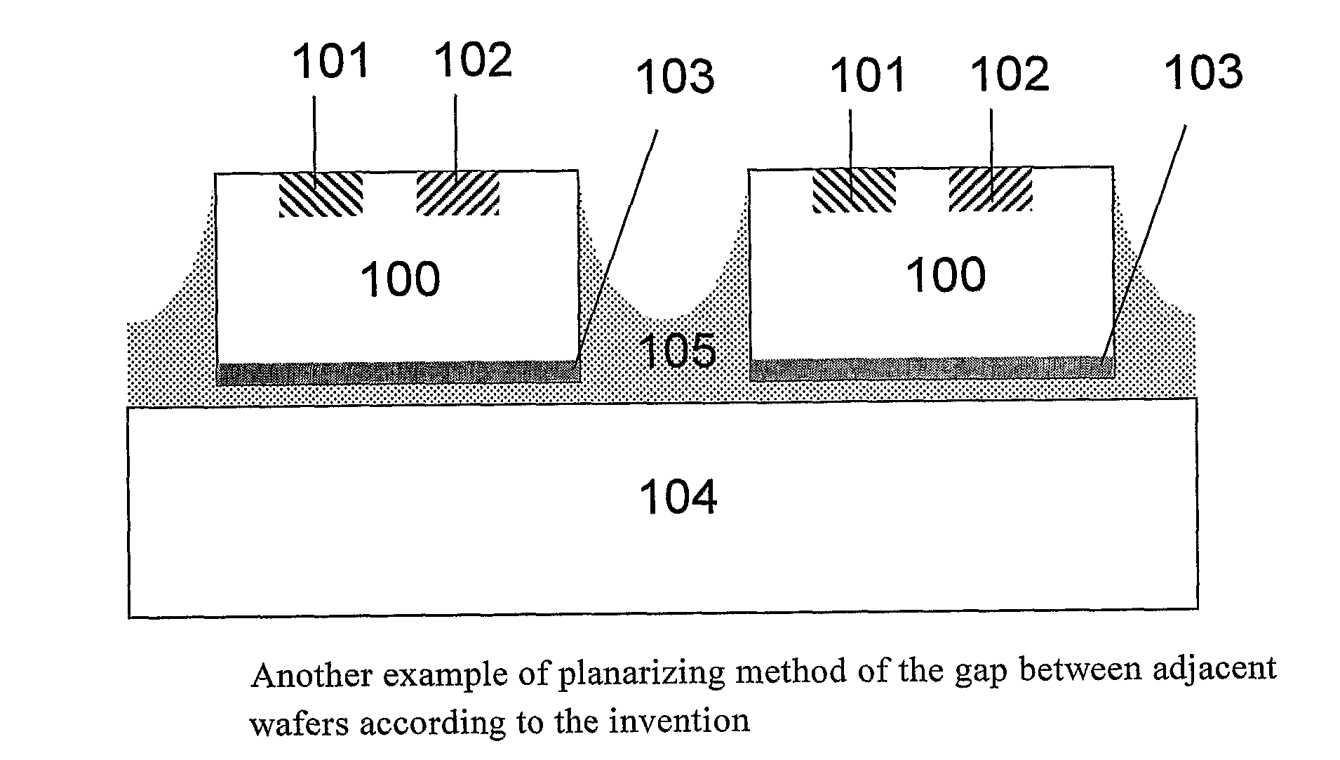
[0030]Similarly, the invention is not tied to use of one or a set of specified patterning of the deposited layer for forming the contacts and interconnects. Any conceivable and known pattern constituting contacts and interconnects may be employed as long as they may be formed on one operation when all the wafers of the solar panel / module are attached onto the transparent front substrate of the panel / module. It might be advantageous to smooth / planarize the edge portion of each wafer to avoid sharp corners or risk of suspending the metal interconnects, and thus avoid risk of breakage and / or short circuiting the interconnects. The edge
smoothing or planarizing may be obtained by removing a part of the front side edge of the wafers, for instance by mechanical or
laser grinding. Alternatively, the
smoothing or planarizing may be obtained by depositing a suitable material along the wafer, or by filling up the space between adjacent wafers to form a more rounded off shape of the edge portion of each wafer. The filling of material may be obtained by conventional techniques such as spin-coat deposition, roller
coating, ink-jet printing, mounting of prefabricated elements etc.
[0037]The wafers may advantageously be planarized, that is the sharp edges of the back side of the wafers may be smoothed, in order to reduce the probability of inducing breakages in the metal bridge formed by the deposited metal layer forming the electric contacts across adjacent wafers. The
smoothing / planarizing of the back side wafer edges may be obtained by, but are not limited to, one of the following process steps: removing a part of the back side edges of the wafers, for instance by
laser ablation, depositing a suitable material along the edges and / or in the space between the wafers to form a smooth, continuous surface in between adjacent wafers, for instance by use of ink-jet printing or mounting of prefabricated elements, or by
coating both the rear surface of the cells and the gaps in between the cells with a
polymer material, preferably with a
polymer material having a high
optical reflectance, having a smoothing effect to surface steps, and deposited for instance by using
spin coating,
spray coating, roller
coating or ink-jet deposition. The removal of the back edges, or filling of material in the gaps between the adjacent wafers, should advantageously result in an angle between the wafer side walls and the transparent substrate of less than 70 degrees, preferably in the range from 30 to 60 degrees. In case of using deposited material, this may be obtained by either by use of ink-jet printing, or by pressing the wafers against the glue on the transparent substrate with a pressure adjusted to obtain glue being squeezed into the spacing between subsequent wafers. The glue should preferably fill up the vertical surface step between the wafer and the transparent substrate by more than 50%, preferably more than 70%, and the
contact angle between the glue and wafer edge surfaces should be less than 70 degrees, preferably in the range 30 to 50 degrees.
[0045]
Metal annealing. An annealing process can be used to improve the metal contact to the underlying
semiconductor and the
conductivity of the metal itself, but has to be sufficiently short and not too hot in order to avoid damaging other elements in the structure, including any glue used to attach the cells to the front glass.



