Method for Adjusting Memory Signal Phase

Active Publication Date: 2011-05-26
SK HYNIX INC
View PDF3 Cites 2 Cited by
  • Summary
  • Abstract
  • Description
  • Claims
  • Application Information

AI Technical Summary

Benefits of technology

[0010]One object of the present invention is to provide a method for adjusting a memory signal phase to reduce phase skew of a signal accessed between a memory controller and a DRAM by accessing and testing the sig

Problems solved by technology

The rising edge and the falling edge of the data strobe signal DQS are present at transitions of the data signal DATA, thus data access errors occur.
Although the DLL adjusts the memory clock signal DCLK to an original extent in response to ambient variations, signal skew may occur in the data access process due to the ambient variations and uncertain factors of hardware components as components or circuits become more complicated, and thus the DLL on the electronic apparatus or the com

Method used


Image

  • Method for Adjusting Memory Signal Phase
  • Method for Adjusting Memory Signal Phase
  • Method for Adjusting Memory Signal Phase

Examples


Example

[0018]In a first embodiment, take a digital audio / video apparatus as an example. An operating system for the digital audio / video is loaded with a program for adjusting the phase of the memory signal in this embodiment to automatically perform phase adjustment according to operation environment and various hardware component characteristics.

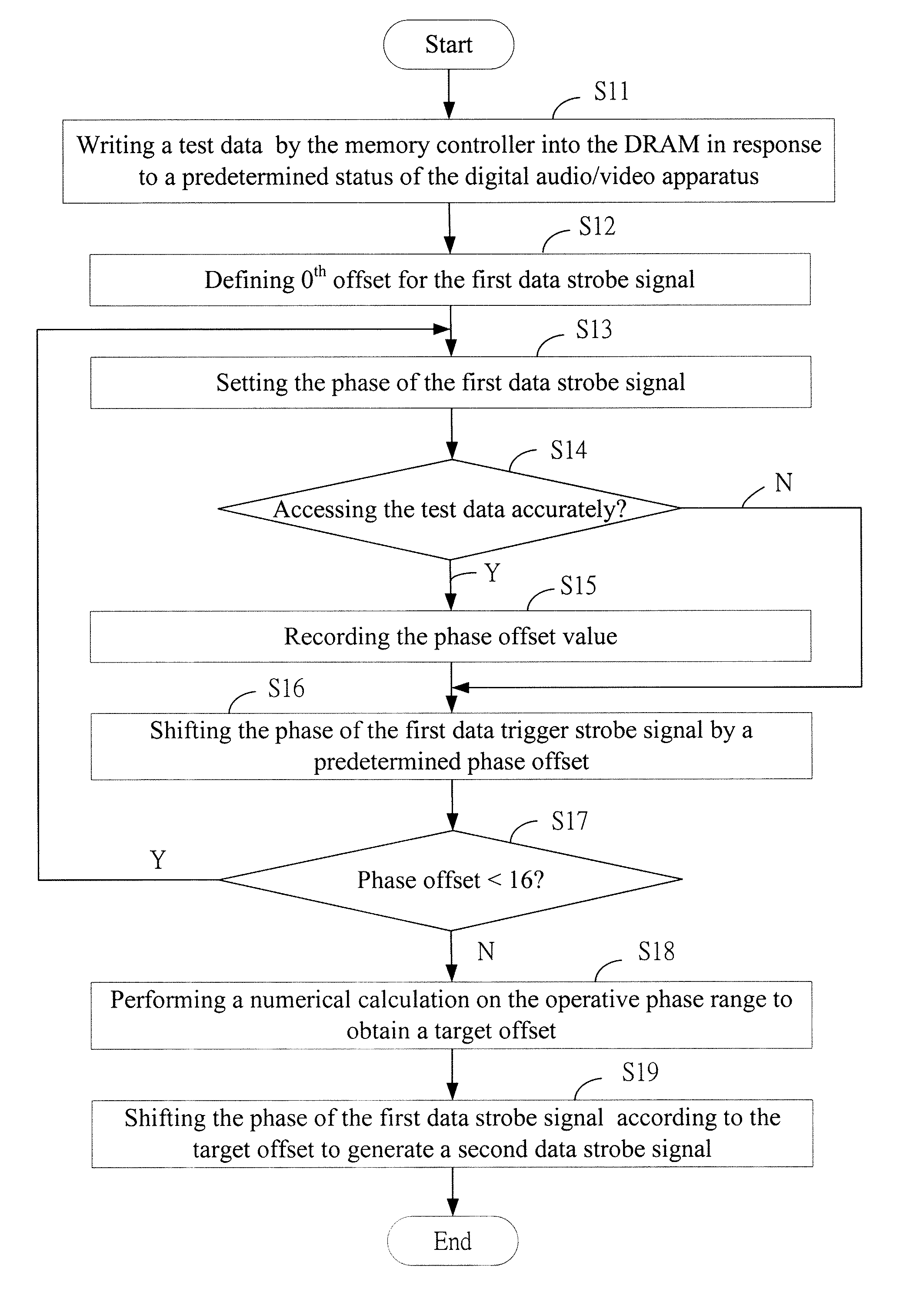
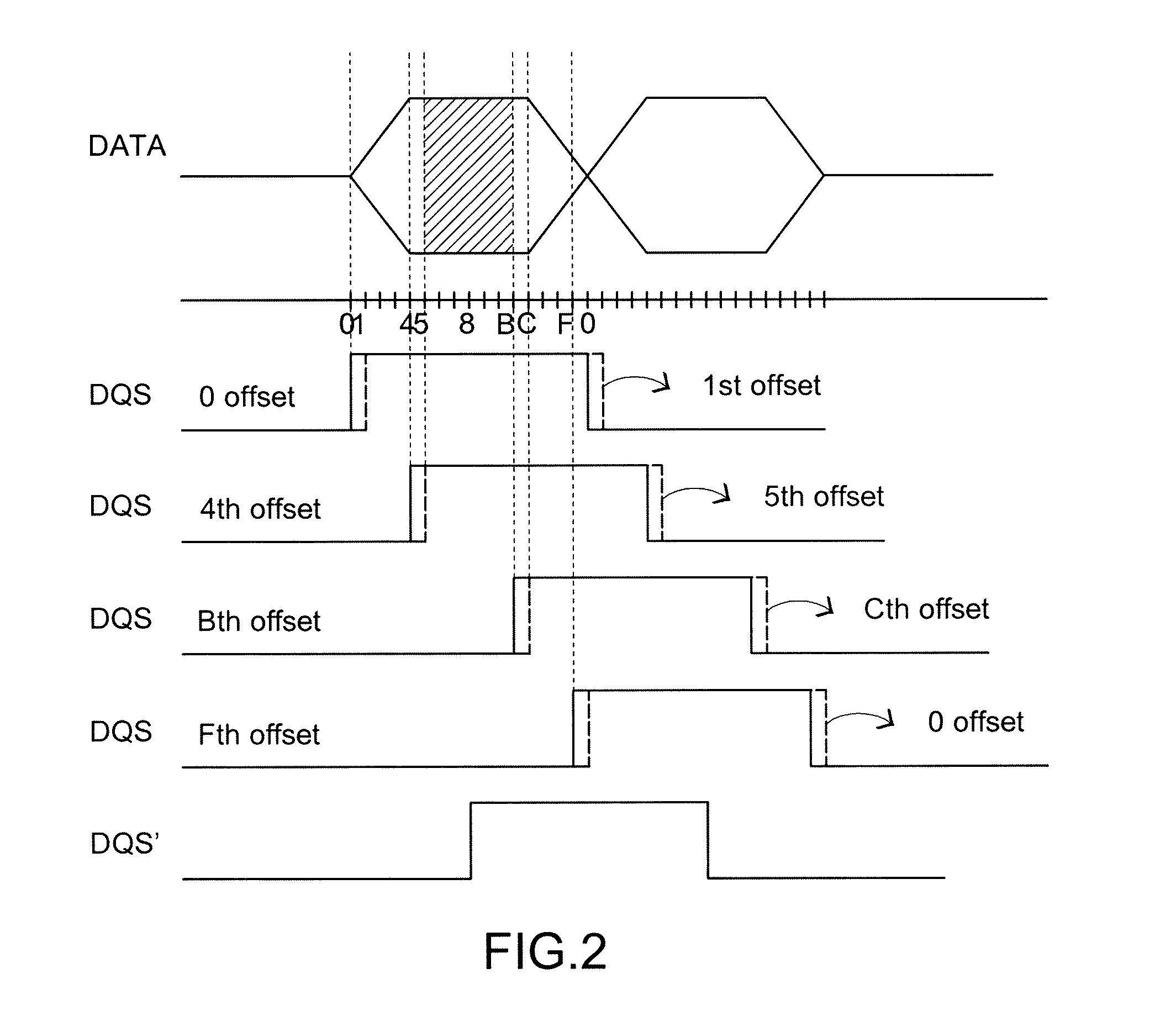
[0019]Please refer to FIG. 2 and FIG. 3. FIG. 2 shows a diagram of continuously adjusting a phase of a first data strobe signal DQS for test data DATA in accordance with the first embodiment of the present invention. FIG. 3 is a flow chart of a method for adjusting the phase of the data strobe signal DQS in accordance with the first embodiment of the present invention.

[0020]In Step S11, in response to a predetermined status of the digital audio / video apparatus, a test data is written by the memory controller into the DRAM. The predetermined status is exemplified by an initial stage for initializing the video apparatus or an operating stage during ...

Example

[0036]In a second embodiment, the complete operative phase range need not be searched for or tested in detail. In other words, 16 times of phase offset need not be completed. Instead, utilizing a hexadecimal register, the phase is continuously offset and the access and verification test is performed on the test data DATA with reference to the first data strobe signal DQS, and only one value of a first phase of the first data strobe signal DQS for accurately accessing data is recorded. For example, referring to FIG. 2, the initial phase of the first data strobe signal DQS represents the first 0th offset, and the first phase value applied to accurately access data occurs at the 5th offset. Further, the digital audio / video apparatus performs a numerical calculation on the 5th offset value. For example, the value 5 representing the 5th offset is added by a predetermined value of 2 or 3, to obtain a target offset value of 7 or 8 and thereby determining the target offset value as a phase ...


PUM


Abstract

A method for adjusting a memory signal phase is applied to data access between a memory controller and a dynamic random access memory (DRAM) of an electronic apparatus. The method includes writing a test data into the DRAM by the memory controller in response to a predetermined status of the electronic apparatus; generating a first data strobe signal; offsetting a phase of the first data strobe signal to access and verify the test data to generate a verification result; generating a target offset value in response to the verification result; and offsetting the phase of the first data strobe signal by the target offset value for subsequent operations.

Description

CROSS REFERENCE TO RELATED PATENT APPLICATION[0001]This patent application is based on Taiwan, R.O.C. patent application No. 098140169 filed on Nov. 25, 2009.FIELD OF THE INVENTION[0002]The present invention relates to a method for adjusting a memory signal phase, and more particularly, to a method for adjusting a signal phase of a dynamic random access memory (DRAM).BACKGROUND OF THE INVENTION[0003]A structure of a main board of a common electronic apparatus or a computer system is composed of a central processing unit (CPU), a control chip, a system memory and peripheral circuits. The control chip controls operations between the CPU and peripheral apparatuses, e.g., data access of the system memory. DRAM, is classified as two types—a synchronous (SDRAM) and a double data rate synchronous dynamic random access memory (DDR SDRAM).[0004]Refer to FIG. 1a showing a block diagram of a memory controller 10 and a system memory 11. For different computer systems, the memory controller 10 m...

Claims


Application Information

Patent Timeline
IPC IPC(8): G06F11/22
CPCG11C29/02G11C29/028G11C29/023G11C29/022
Inventor CHIANG, YUNG CHIH
Owner SK HYNIX INC
Why Eureka
Try Eureka