Electronic Component Device and Method for Manufacturing the Same

a technology of electronic components and manufacturing methods, applied in the direction of coupling device connections, electrical apparatus casings/cabinets/drawers, soldering apparatus, etc., can solve the problems of high production cost, low productivity, and impair the quality of electronic circuit forming, so as to reduce production costs and shorten heating and bonding time, the effect of rapid growth ra

Active Publication Date: 2011-06-09
MURATA MFG CO LTD
View PDF12 Cites 59 Cited by
  • Summary
  • Abstract
  • Description
  • Claims
  • Application Information

AI Technical Summary

Benefits of technology

[0027]In accordance with the present invention, since the Ni—Bi alloy formed at the bonding section has a rapid growth rate as compared with Cu3Sn described above, the bonding section can be formed in a short time and production cost can be reduced. Since a time for heating and bonding can be shortened, a thermal load on the electronic component device can be reduced and therefore, it becomes possible to apply the present invention to electronic component devices which are vulnerable to a high-temperature load.
[0028]Further, in accordance with the present invention, it is possible to prevent the alloy formed at the bonding section from melting, for example, in a solder reflow step since the Ni—Bi alloy has a relatively high melting point, for example, 469° C. for NiBi3 and 654° C. for NiBi. Accordingly, the hermeticity of the electronic component device is not impaired even after the solder reflow step.
[0029]In the present invention, when the bonding section is formed so as to

Problems solved by technology

Therefore, this process leads to a problem that productivity is low and production cost is high.
Further, the above-mentioned conditions may be extreme conditions of impairing the quality of the electronic circ

Method used


Image

  • Electronic Component Device and Method for Manufacturing the Same
  • Electronic Component Device and Method for Manufacturing the Same
  • Electronic Component Device and Method for Manufacturing the Same

Examples


first embodiment

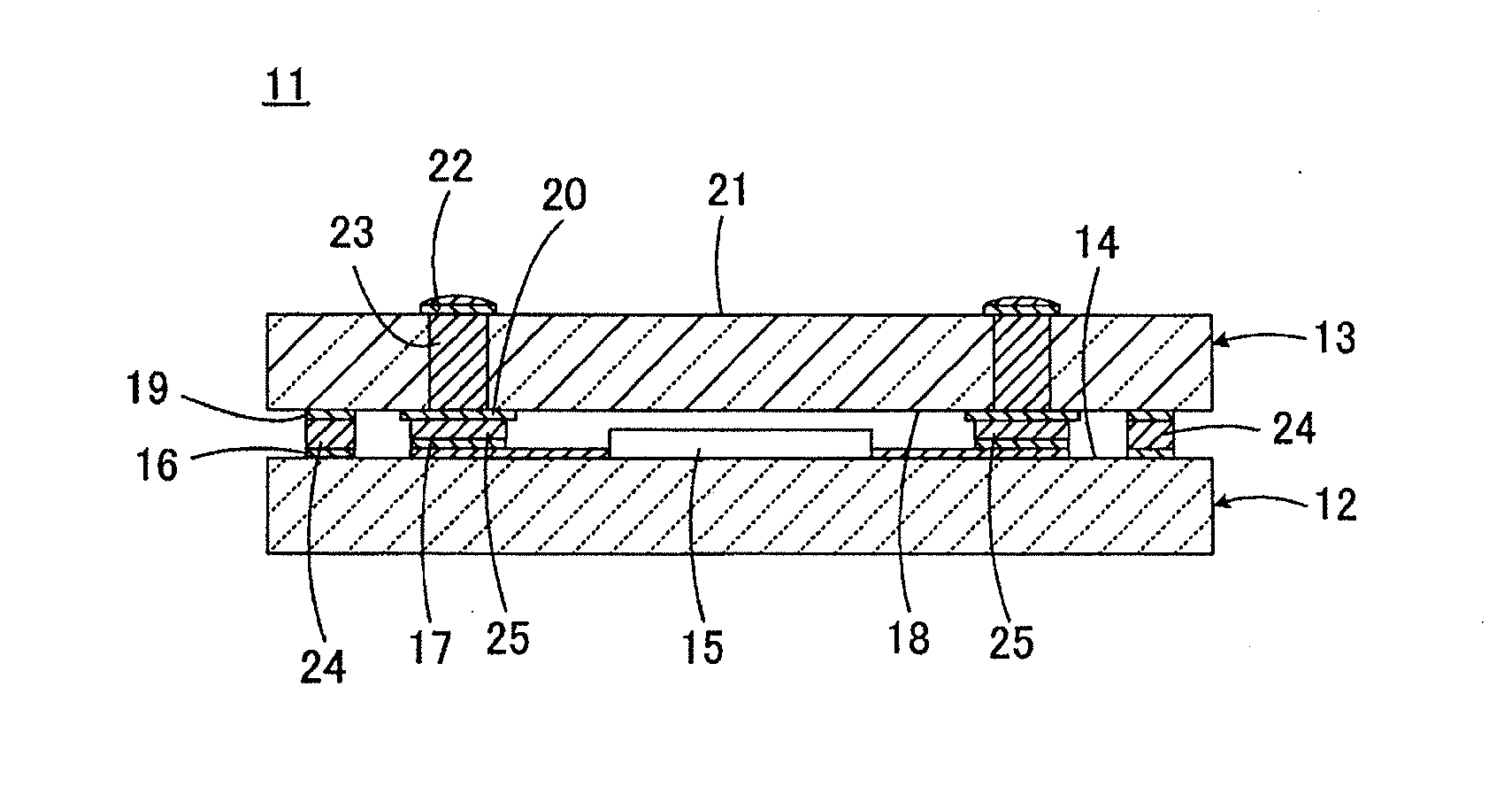
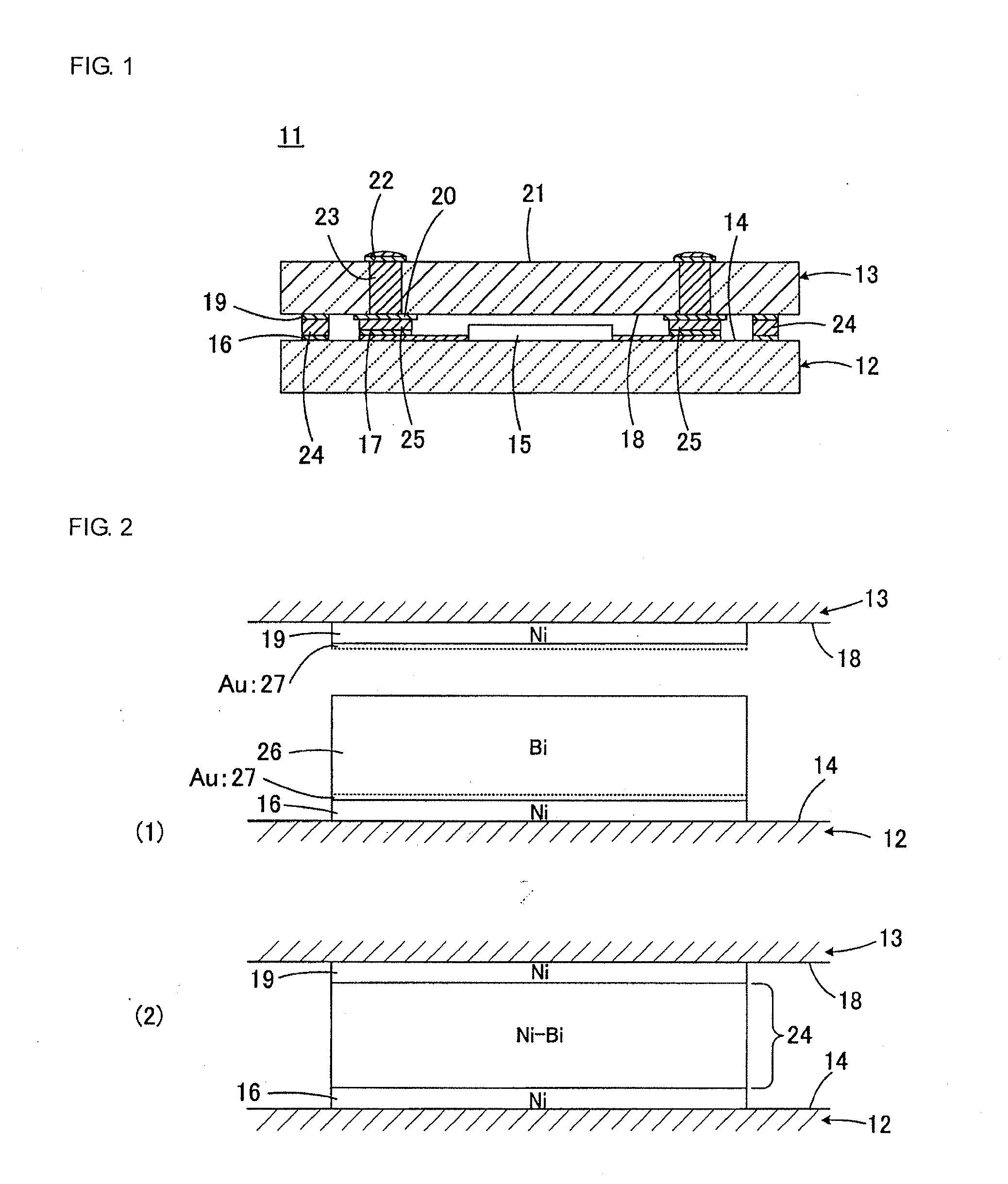
[0049]FIG. 2 is a view for illustrating the present invention and shows an enlarged view of a part of the first sealing frame 16 and a part of the second sealing frame 19 in FIG. 1. FIG. 2(1) shows a pre-bonding state and FIG. 2(2) shows a post-bonding state of the first sealing frame 16 and the second sealing frame 19.

[0050]With reference to FIG. 2(1), both of the first sealing frame 16 and the second sealing frame 19 are composed of a Ni film predominantly composed of Ni. Each of the widths of the first and second sealing frames 16 and 19 is, for example, 50 μm. In addition, in order to enhance adhesion between the Ni film and each of the main substrate 12 and the cover substrate 13, a Ti film, but not shown, may be formed between the Ni film and the main substrate 12 and between the Ni film and the cover substrate 13.

[0051]A Bi layer 26 predominantly composed of Bi is formed on the first sealing frame 16. An oxidation resistant film 27 composed of Au is formed between the first s...

second embodiment

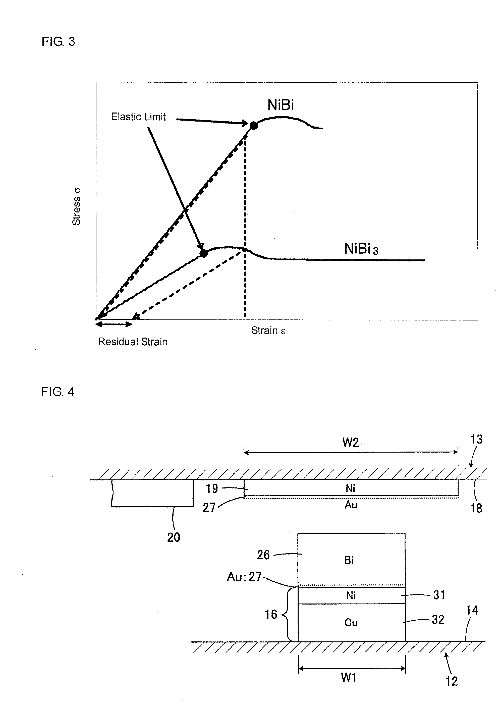
[0067]FIG. 4 is a view corresponding to FIG. 2(1) for illustrating the present invention. In FIG. 4, the same reference symbols are given to elements corresponding to the elements shown in FIG. 2, and overlapped descriptions are omitted.

[0068]The second embodiment has a feature that a dimension W2 in the width direction of the second sealing frame 19 is larger than a dimension W1 in the width direction of the first sealing frame 16. This is a configuration for preventing Bi constituting the Bi layer 26 from protruding from the first sealing frame 16 due to the pressurization in the heating and bonding step to cause electric short circuit between the protruded Bi and the connecting electrode 20, for example. As an example, when the dimension W2 in the width direction of the second sealing frame 19 is 50 μm, the dimension W1 in the width direction of the first sealing frame 16 is set at about 15 to 25 μm.

[0069]In addition, in the embodiment shown in FIG. 4, the first sealing frame 16,...

third embodiment

[0076]Further, a cap-shaped substrate shown in FIG. 5 may be used for the cover substrate. FIG. 5 is a view for illustrating the present invention and a perspective view showing a main substrate 42 and a cover substrate 43 included in an electronic component device 41 separately. FIG. 6 is an enlarged sectional view of a bonding section of the main substrate 42 and the cover substrate 43 shown in FIG. 5. In FIG. 5, the same reference symbols are given to elements corresponding to the elements shown in FIG. 2(1), and overlapped descriptions are omitted.

[0077]On an upper main surface 14 of the main substrate 42, an element 44 to form a required circuit is mounted and the first sealing frame 16 surrounding the element 44 is formed. In addition, a connecting conductor to be lead out of the element 44 is omitted in FIG. 6.

[0078]On the other hand, a recessed section 46 (refer to FIG. 6) is formed on a lower main surface of the cap-shaped cover substrate 43, and the second sealing frame 19...


PUM

PropertyMeasurementUnit
Temperatureaaaaaaaaaa
Fractionaaaaaaaaaa
Timeaaaaaaaaaa

Abstract

An electronic component device having a first sealing frame formed on a main substrate and a second sealing frame formed on a cover substrate, the first and second sealing frames being composed of a Ni film. A bonding section constituted by a Ni—Bi alloy is formed between the first and second sealing frames. For example, a Bi layer is formed on the first sealing frame, and then the first sealing frame and the second sealing frame are heated at a temperature of 300° C. for at least 10 seconds while applying pressure in the direction in which the first sealing frame and the second sealing frame are in close contact with each other, and thus the bonding section, which bonds the first sealing frame to the second sealing frame, is formed.

Description

CROSS REFERENCE TO RELATED APPLICATIONS[0001]The present application is a continuation of International Application No. PCT / JP2009 / 064156, filed Aug. 11, 2009, which claims priority to Japanese Patent Application No. JP2008-212471, filed Aug. 21, 2008, the entire contents of each of these applications being incorporated herein by reference in their entirety.FIELD OF THE INVENTION[0002]The present invention relates to an electronic component device and a method for manufacturing the same, and particularly to an electronic component device having a structure of bonding sealing frames to each other for hermetic sealing, and a method for manufacturing the same.BACKGROUND OF THE INVENTION[0003]Electronic component devices of interest to the present invention include, for example, a BAW filter. The BAW filter includes a main substrate provided with an electronic circuit forming section and a first sealing frame surrounding the electronic circuit forming section on one main surface of the ...

Claims


Application Information

Patent Timeline
IPC IPC(8): H01R13/46H05K3/00
CPCB23K1/0016H01L23/10H01L2924/01079H05K13/00Y10T29/49124H01L2924/0002B32B15/018B32B15/01H01L2924/00Y10T29/49121Y10T29/4913Y10T29/49144
Inventor HORIGUCHI, HIROKIKIMURA, YUJI
Owner MURATA MFG CO LTD
Why Eureka
Try Eureka