Atomic layer etching with pulsed plasmas

a plasma etching and atomic layer technology, applied in the direction of electrical discharge tubes, decorative arts, electrical equipment, etc., can solve the problems of etching process self-limiting, substrate removal with traditional alet processes requires a very long etching cycle, and the etching cycle is approaching and exceeding 150 seconds per cycl

Inactive Publication Date: 2011-06-16
UNIV HOUSTON SYST
View PDF12 Cites 610 Cited by
  • Summary
  • Abstract
  • Description
  • Claims
  • Application Information

AI Technical Summary

Benefits of technology

[0014]The foregoing has outlined rather broadly the features and technical advantages of the invention in order that the detailed description of the invention that follows may be better understood. Additional features and advantages of the invention will be described hereinafter that form the subject of the claims of the invention.

Problems solved by technology

Ideally, this process is also self-limiting; ions react only with substrate atoms bonded to the chemisorbed gas.
Once the chlorinated layer is removed, further etching by physical sputtering of the substrate must not occur or be sufficiently limited.
However, the achievement of nearly atomic monolayer, substrate removal with traditional ALET processes requires a very long etching cycle, approaching and exceeding 150 seconds per cycle.
Further, traditional ALET processes include additional limitations.
First, gas pulsing is a disadvantage, exacerbated by the fact that chemisorption gases, such as Cl2, have a long residence time on the chamber walls and require long pumping periods before the inert gas plasma is ignited.
This makes the etching rate very slow, even for the times required to etch very thin films.
Second, the etching rate per cycle may not necessarily be constant or controllable.
Present plasma etching processes are too coarse to achieve such precise pattern transfer and can damage underlying layers of the substrate.
In particular, traditional plasma etching techniques do not have the level of control that is needed for precise patterning of sub-20 nm structures and the current atomic layer etching with pulsed gases is too slow to be practical for large volume manufacturing of future integrated circuits.
Additionally, the current techniques require an excess of precursor raw materials, such as chlorine gas, which represents potential cost reductions for finding more efficient processes.

Method used


Image

  • Atomic layer etching with pulsed plasmas
  • Atomic layer etching with pulsed plasmas
  • Atomic layer etching with pulsed plasmas

Examples


examples

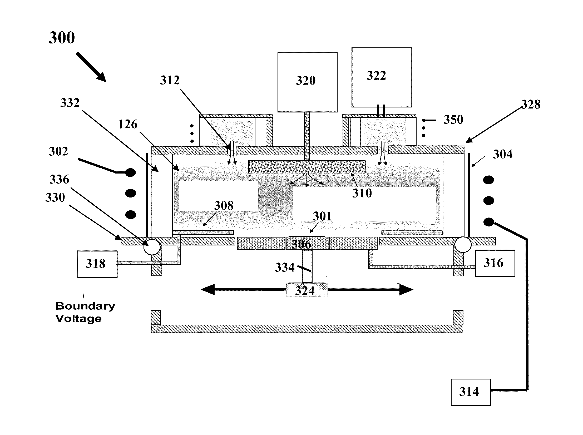
[0085]Experimental apparatus: FIGS. 3 and 6 show schematics of the experimental apparatus used in this study. The inductively coupled plasma (ICP) was ignited by a 3-turn spiral coil in a 17.8 cm long, 8.6 cm inside diameter alumina tube. A copper Faraday shield prevented capacitive coupling between the coil and the plasma. The discharge tube was connected to a cubical stainless steel (SS) chamber through an adaptor flange. A water channel in that flange served to cool the Faraday shield and prevent overheating of the discharge tube. The system was pumped by a 300 l / s turbo pump backed by a dry pump. Pressure was measured by a MKS 629 capacitance manometer mounted downstream of the plasma at 0.1 Torr full scale setting. A calibration experiment, without plasma, showed that the pressure at the discharge region was about 30-40% higher than that measured at the position of the pressure gauge. Pressures reported below are all calibrated values and refer to the plasma region.

[0086]A stai...


PUM

PropertyMeasurementUnit
DC voltagesaaaaaaaaaa

Abstract

A system and method for rapid atomic layer etching (ALET) including a pulsed plasma source, with a spiral coil electrode, a cooled Faraday shield, a counter electrode disposed at the top of the tube, a gas inlet and a reaction chamber including a substrate support and a boundary electrode. The method includes positioning an etchable substrate in a plasma etching chamber, forming a product layer on the surface of the substrate, removing a portion of the product layer by pulsing a plasma source, then repeating the steps of forming a product layer and removing a portion of the product layer to form an etched substrate.

Description

CROSS-REFERENCE TO RELATED APPLICATIONS[0001]This application claims benefit under 35 USC §119 of U.S. provisional application No. 61 / 286,572 filed Dec. 15, 2009, entitled “Atomic Layer Etching with Pulsed Plasmas” which is hereby incorporated herein by reference in its entirety for all purposes.STATEMENT REGARDING FEDERALLY SPONSORED RESEARCH OR DEVELOPMENT[0002]The U.S. Government has a paid-up license in this invention and the right in limited circumstances to require the patent owner to license others on reasonable terms as provided for by the terms of Grant Nos. DE-P502-09ER09-01 awarded by the U.S. Department of Energy and CBET-0903426 awarded by the National Science Foundation.BACKGROUND OF THE INVENTION[0003]1. Field of the Invention[0004]The present disclosure relates to a nanofabrication process. More specifically, the present disclosure relates to new cyclic process for etching a solid surface with atomic layer precision.[0005]2. Background of the Invention[0006]Atomic la...

Claims


Application Information

Patent Timeline
Patent Type & Authority Applications(United States)
IPC IPC(8): C23F1/00C23F1/08
CPCH01J37/32036H01J37/32045H01L21/3065H01J37/32146H01J37/32174H01J37/32082H01L21/30655
Inventor DONNELLY, VINCENT M.ECONOMOU, DEMETRE J.
Owner UNIV HOUSTON SYST
Why Eureka
Try Eureka