[0013]The present invention provides device component geometries and fabrication strategies for enhancing the electronic performance of electronic devices based on thin films of randomly oriented or partially aligned semiconducting nanotubes. In certain aspects, devices and methods of the present invention incorporate a patterned layer of randomly oriented or partially aligned carbon nanotubes, such as one or more interconnected SWNT networks, providing a
semiconductor channel exhibiting improved
electronic properties relative to conventional
nanotube-based
electronic systems.
[0014]Embodiments of this aspect include, for example, electronic devices and device components comprising a patterned layer of randomly oriented or partially aligned carbon nanotubes having void regions, such as etched regions, channels and / or cavities in the
nanotube layer, that reduce the number and extent of purely metallic conductive pathways between electrodes of an electronic device. Methods and devices of certain aspects reduce the number and extent of purely metallic conductive pathways in one or more interconnected
carbon nanotube networks so as to access
nanotube-based transistors exhibiting improved on / off ratios and decreased static
power consumption. In specific embodiments, void regions are patterned into a
monolayer or sub-
monolayer film of randomly oriented or partially aligned nanotubes, for example by
photolithography and
etching methods, that define a plurality of physically isolated or interconnected strips comprising interconnected
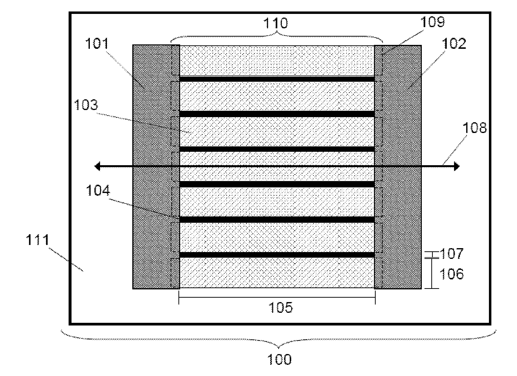
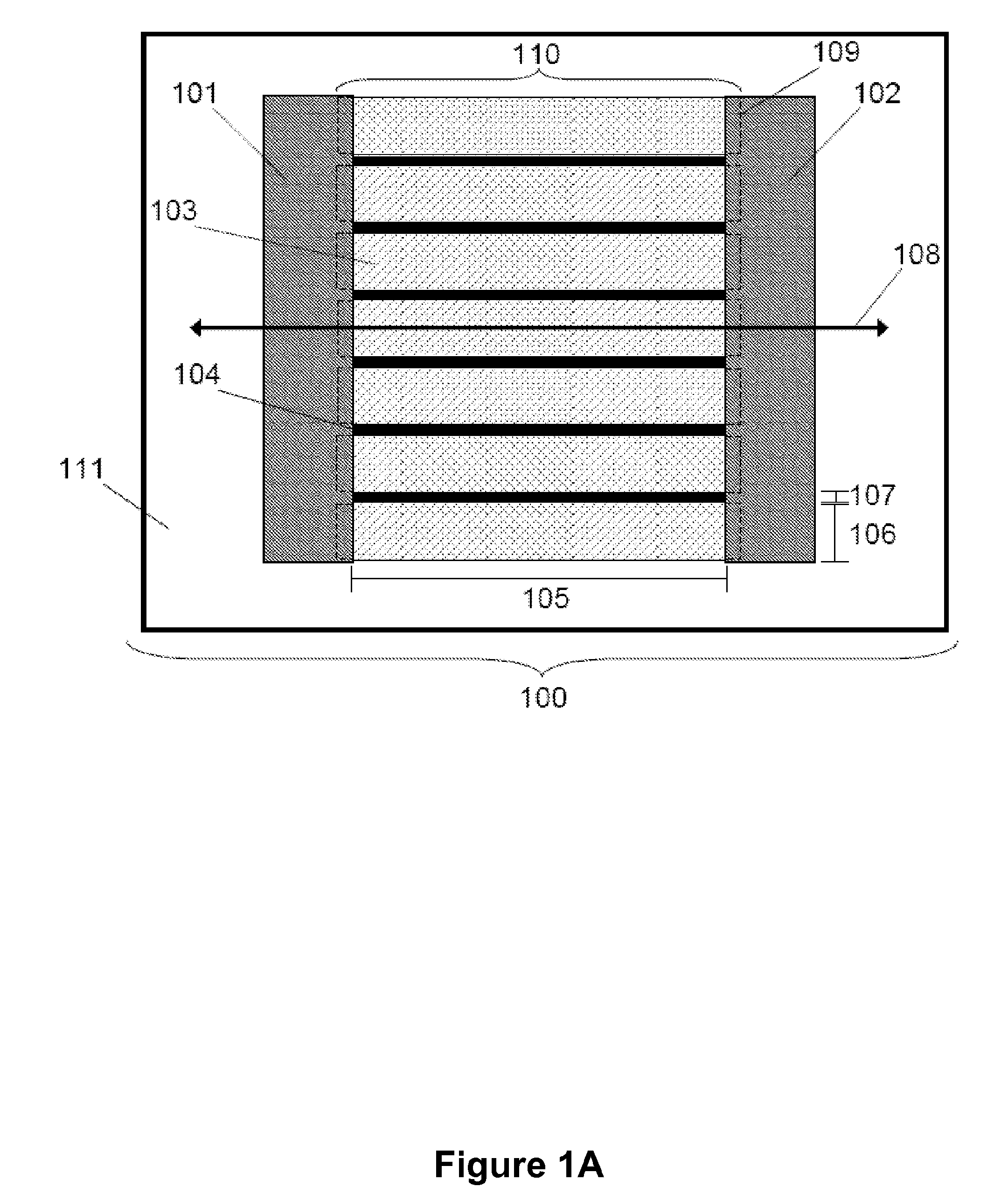
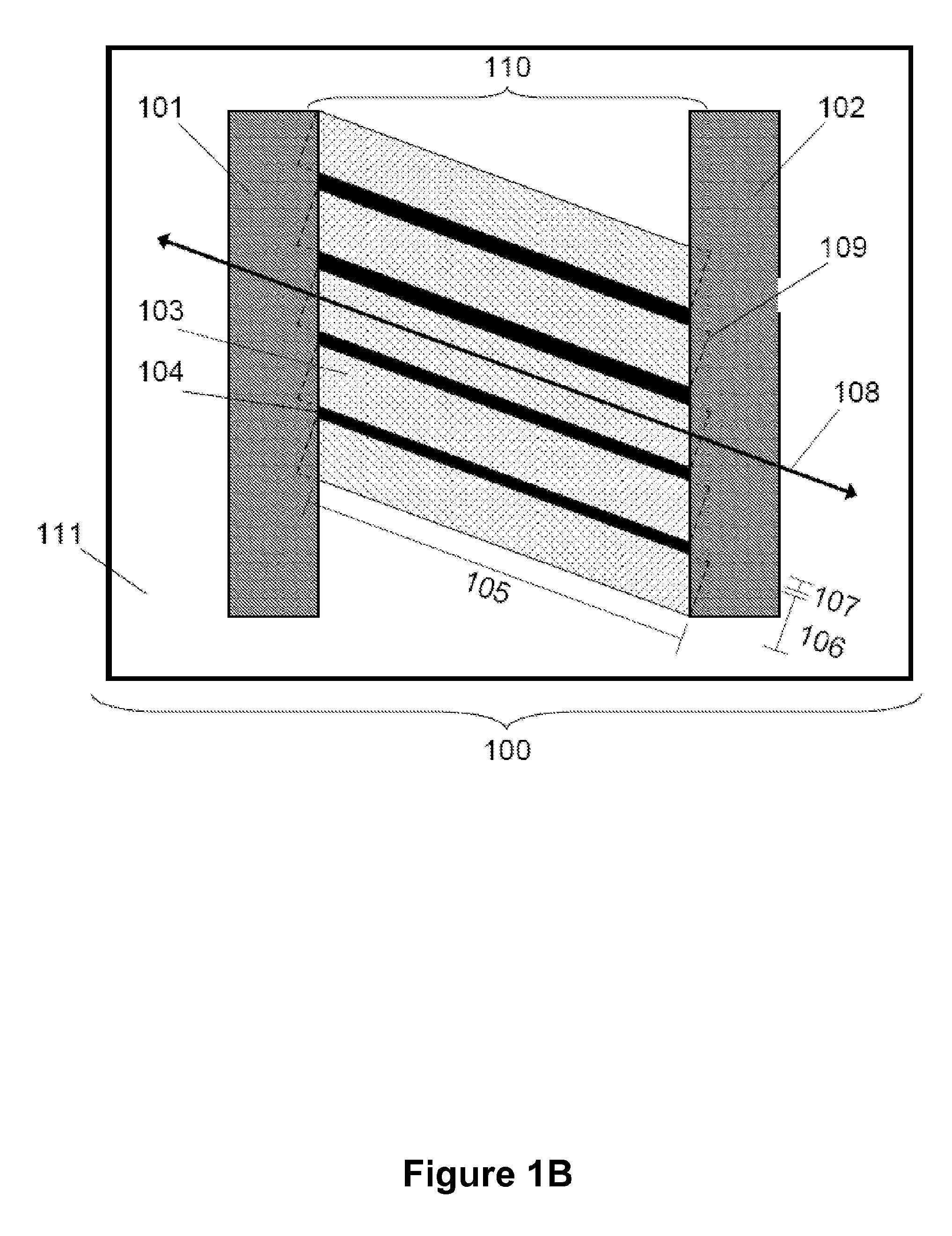
carbon nanotube networks (e.g., bands of interconnected nanotube networks). In some embodiments, strips are provided, for example, comprising discrete bands of interconnected carbon nanotube networks that extend lengths from the first
electrode to the second
electrode. Optionally, each of the bands extend an average width in a dimension orthogonal to the average length, wherein the average width of the band is less than the length of the strip, for example, 10 times less or preferably for some embodiments 50 times less or preferably for some embodiments 100 times less. As semiconducting SWNTs are more abundant than metallic SWNTs in the nanotube layer, the formation of strips by patterning voids in the
interconnection carbon nanotube network effectively limits the extent and number of purely metallic conductive pathways between the source and drain electrodes of the
transistor. Accordingly, the patterned nanotube layer device geometries of the present invention provide an effective means of increasing device on / off ratios by at least an
order of magnitude (and in some embodiments up to 4 orders of magnitude) while only slightly impacting the overall effective device mobility of these systems.
[0015]The present fabrication methods and device geometries are versatile, thereby providing a platform enabling a new class of nanotube-based electronic devices and systems well suited for a range of device applications, including thin film
electronics, large area
electronics (e.g., macroelectronics),
flexible electronics, and sensing. Methods and devices of the present invention are compatible with low temperature, solution-based
processing and
assembly on a wide range of device substrates, including mechanically flexible substrates such as
polymer substrates.
Processing methods and design strategies of the present invention are complementary to conventional
microfabrication and nanofabrication platforms, and can be effectively integrated into existing photolithographic,
etching and thin film deposition patterning strategies, systems and infrastructure. In specific embodiments, methods and device geometries of the present invention enable low cost fabrication of high performance nanotube based
semiconductor devices, such as thin film transistors,
transistor arrays, and integrated electronic circuits.

