Method of Etching Oxide Layer and Nitride Layer

Active Publication Date: 2011-06-23
UNITED MICROELECTRONICS CORP
View PDF6 Cites 0 Cited by
  • Summary
  • Abstract
  • Description
  • Claims
  • Application Information

AI Technical Summary

Benefits of technology

[0008]Accordingly, the present invention is directed to a method of etching an oxide layer and a nitride layer, to effectively remove a redundant fence on a surface of wafer and thereby the above-mentioned problems of the prior art may be resolved.
[0011]Since the present invention uses the complex hard mask including nitride layer and oxide layer, the redundant fence may be effectively removed due to different etching selectivity of the nitride layer and the oxide layer. Therefore, layout patterns of the active device may be more accurately controlled and the performance of the active device may be effectively improved.

Problems solved by technology

However, during fabrication process of the SONOS structure, it is found that sidewalls of a shallow trench isolation (STI) structure that protrude out of a surface of wafer usually have unwanted residual material layer forming a redundant fence (termed as sidewall residual or redundant spacer).
The influence caused by the redundant fence can not be eliminated by adjusting the position of the implantation mask or the direction of the implantation process.
In other words, the redundant fence would cause reduction in the effective area of active region, especially for a narrow width device.
Even more, the redundant fence would cause decrease in current of the narrow width device and thus adversely influence the operation of the narrow width device.
If a process time of the etching process is prolonged, an additional isotropic etching process is required, or an additional anisotropic etching process is required in order to remove the redundant fence, which may seriously damage the other material layers or components on the surface of wafer.
For example, a serious side effect may therefore damage the SONOS structure.
The fabrication and operation of the device may be worse due to such an additional etching process.

Method used


Image

  • Method of Etching Oxide Layer and Nitride Layer
  • Method of Etching Oxide Layer and Nitride Layer
  • Method of Etching Oxide Layer and Nitride Layer

Examples


Embodiment Construction

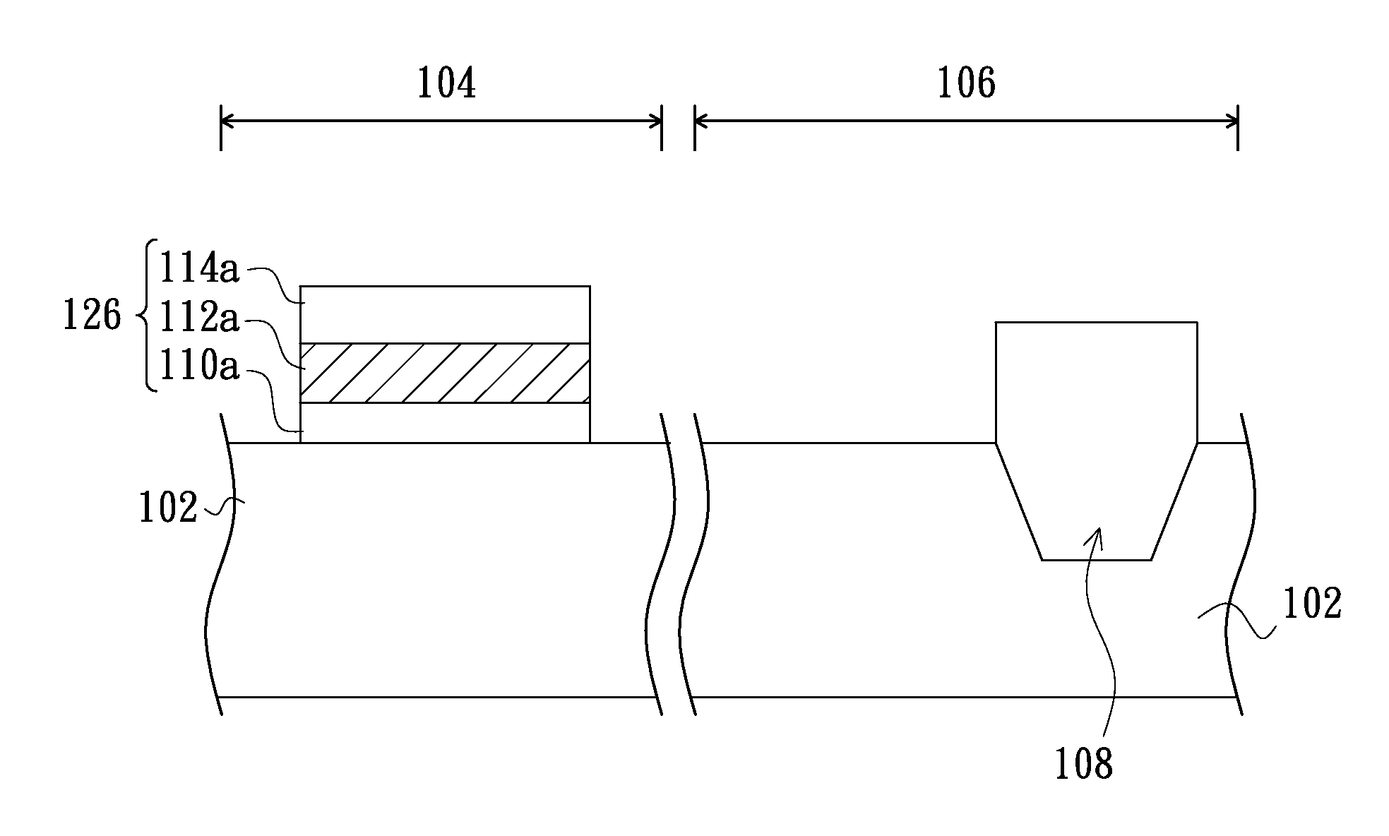
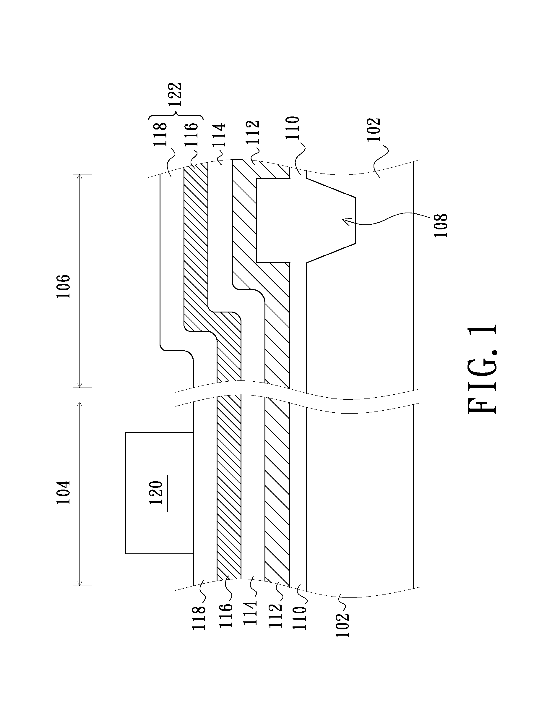
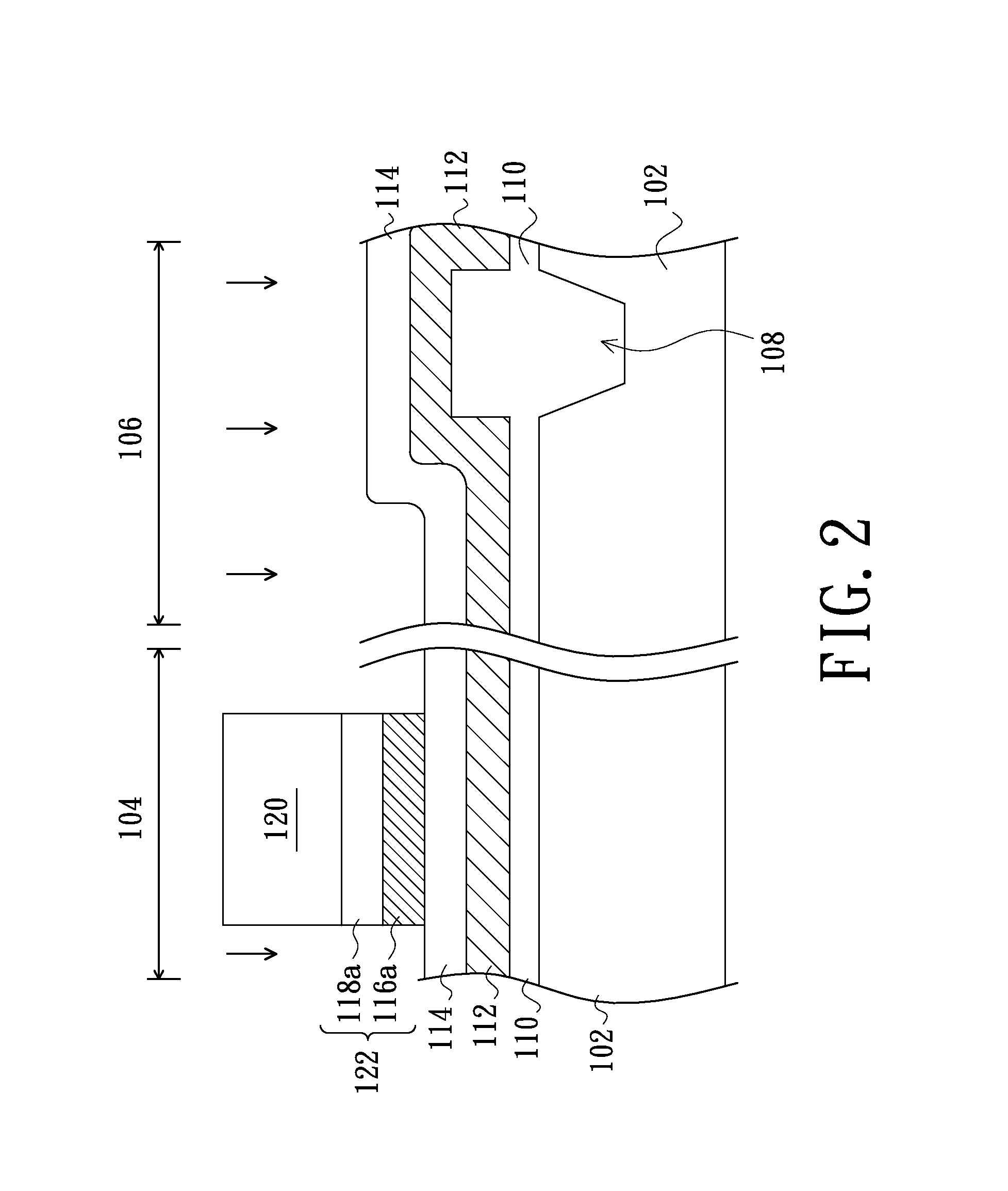
[0014]Hereinafter, an embodiment of the present invention will be described in detail with reference to the accompanying drawings. Here, it is to be noted that the present invention is not limited thereto. Furthermore, the step serial numbers concerning the saturation adjustment method are not meant thereto limit the operating sequence, and any rearrangement of the operating sequence for achieving same functionality is still within the spirit and scope of the invention.

[0015]Referring to FIGS. 1 through 7, FIGS. 1-7 illustrate schematic views associated with a method of etching an oxide layer and a nitride layer in accordance with an embodiment of the present invention. In the drawings, same or like components or parts are designated by the same reference numerals. It is to be understood that the drawings are not drawn to scale and are served only for illustration purposes. As illustrated in FIG. 1, a substrate 102, for example, comprised of a silicon substrate, a silicon-containing...


PUM


Abstract

An exemplary method of patterning oxide layer and removing residual nitride includes steps of forming a first oxide layer, a nitride layer, a second oxide layer and a complex hard mask on a substrate in turn. The first oxide layer covers an insulating structure. The second oxide layer, the complex hard mask and the nitride layer are etched by utilizing a patterned photoresist as an etching mask, so as to expose the first oxide layer. In addition, the part of the nitride layer covering the insulating structure can be further removed. Accordingly, the present invention can effectively control layout patterns of material layers and doped regions and thereby can improve the performance of a narrow width device.

Description

BACKGROUND[0001]1. Technical Field[0002]The present invention generally relates to a method of etching an oxide layer and a nitride layer, and more particularly to a method of forming an oxide-nitride-oxide (ONO) structure.[0003]2. Description of the Related Art[0004]Usually, there are many applications of nitride and oxide within integrated circuits (ICs), for example, an isolation structure between adjacent transistors, a gate spacer, an etch stop layer, a protection layer for outermost layer of IC chip, an ONO structure, etc.[0005]A non-volatile static random access memory (nvSRAM) is taken as an example. The nvSRAM generally includes a static random access unit and a non-volatile memory unit. The static random access unit is applied for temporarily accessing data when a power is supplied. The non-volatile memory unit is capable of storing data even when the power supply to it is cut off. The nvSRAM uses a silicon-oxide-nitride-oxide-silicon (SONOS) structure formed therein as a ...

Claims


Application Information

Patent Timeline
IPC IPC(8): H01L21/306H01L21/314
CPCH01L21/28282H01L21/31144H01L21/31133H01L29/40117
Inventor SHIH, PING-CHIA
Owner UNITED MICROELECTRONICS CORP
Why Eureka
Try Eureka