

Smooth siconi etch for silicon-containing films
a silicon-containing film and smooth siconi technology, applied in decorative arts, electrical equipment, electrical discharge tubes, etc., can solve the problems of difficult to realize the effect of etching silicon, difficult to achieve etching, and difficulty in reducing the size of solid by-products, so as to reduce the roughness of the post-etch surface and reduce the difference in etching rate. , the effect of reducing the flow ratio of hydrogen
- Summary
- Abstract
- Description
- Claims
- Application Information
AI Technical Summary
Benefits of technology
Problems solved by technology
Method used
Image

Examples
Embodiment Construction
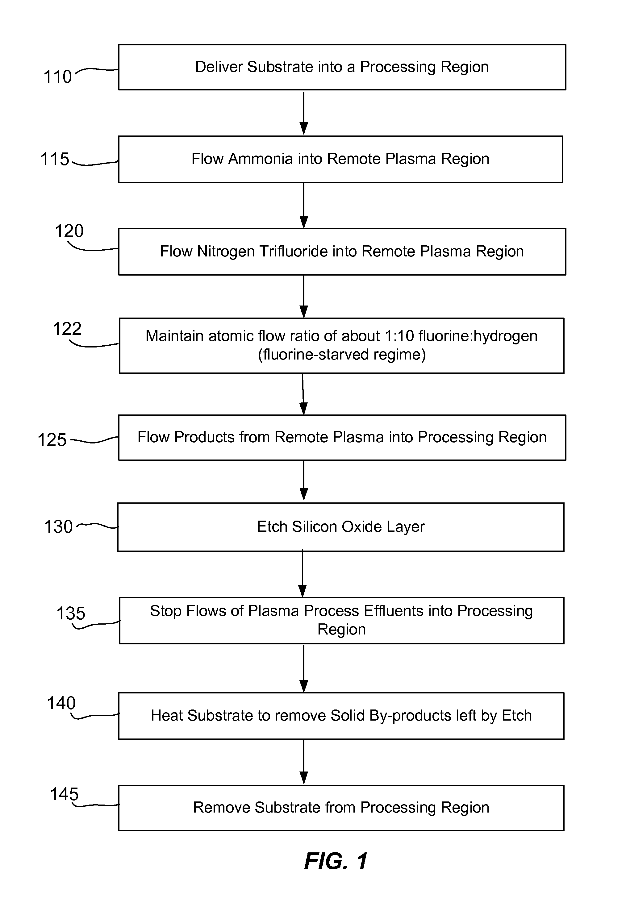
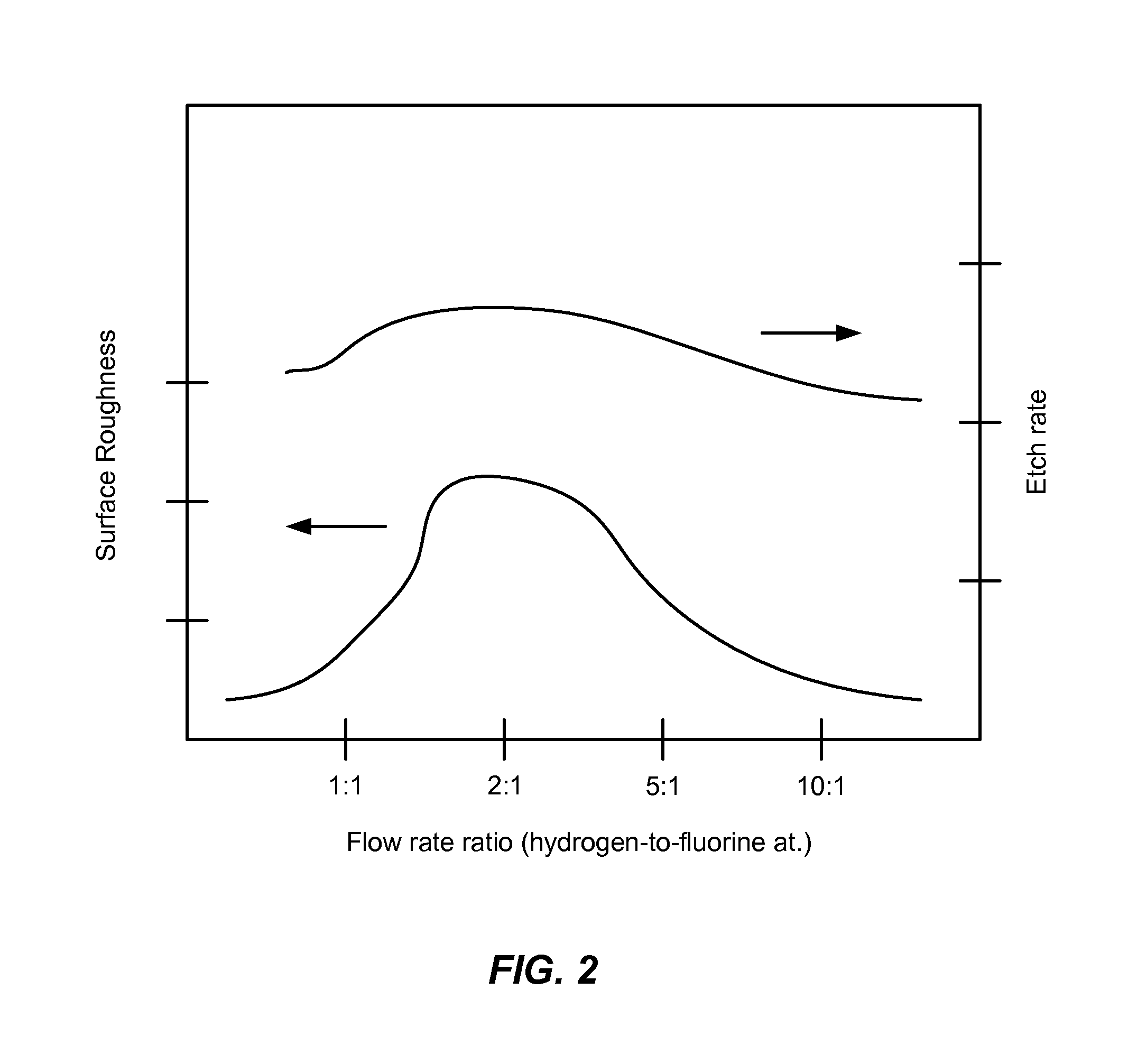
[0021]A method of etching silicon-containing material is described and includes a SiConi™ etch having a greater or lesser flow ratio of hydrogen compared to fluorine than that found in the prior art. Modifying the flow rate ratios in this way has been found to reduce roughness of the post-etch surface and to reduce the difference in etch-rate between densely and sparsely patterned areas. Alternative means of reducing post-etch surface roughness include pulsing the flows of the precursors and / or the plasma power, maintaining a relatively high substrate temperature and performing the SiConi™ in multiple steps. Each of these approaches, either alone or in combination, serve to reduce the roughness of the etched surface by limiting solid residue grain size.
[0022]SiConi™ etch processes have used a hydrogen source of ammonia (NH3) and a fluorine source of nitrogen trifluoride (NF3) which together flow through a remote plasma system (RPS) and into a reaction region. In the past, SiConi™ et...
PUM
| Property | Measurement | Unit |
|---|---|---|
| Temperature | aaaaa | aaaaa |
| Fraction | aaaaa | aaaaa |
| Fraction | aaaaa | aaaaa |
Abstract
Description
Claims
Application Information