Method for producing group III nitride semiconductor

a technology of nitride and semiconductor, which is applied in the direction of single crystal growth, polycrystalline material growth, liquid-phase epitaxial layer growth, etc., can solve the problem of cumbersome second method, and achieve the effect of preventing the generation of cracks, and reducing the number of steps

Active Publication Date: 2011-06-30
TOYODA GOSEI CO LTD
View PDF4 Cites 12 Cited by
  • Summary
  • Abstract
  • Description
  • Claims
  • Application Information

AI Technical Summary

Benefits of technology

[0029]According to the first aspect of the invention, the second Group III nitride semiconductor layer which has been grown by the flux method and which has a c-plane as a main plane can be readily separated from the sapphire substrate without generating cracks in the semiconductor layer.
[0030]According to the second aspect, the present invention is advantageous in the case where the second Group III nitride semiconductor layer is grown through the flux method to a thickness of 0.5 mm or more. When the thickness is 0.5 mm or more in a simple deposition, the stress generated due to the differences in linear expansion coefficient and lattice constant between sapphire and GaN increases, to thereby readily generate cracks in the GaN layer. However, according to the present invention, generation of cracks can be effectively prevented in the growing second Group III nitride semiconductor, whereby a crack-free second Group III nitride semiconductor layer having a thickness of 0.5 mm or more can be readily produced.
[0031]According to the third aspect of the invention, through controlling only pressure, the conditions where crystal growth of the Group III nitride semiconductor is inhibited can be shifted to the conditions where crystal growth of the Group III nitride semiconductor is permitted. Particularly, according to the fourth aspect of the invention, the first step can be shifted to the second step through controlling only pressure, whereby the production steps can be streamlined.
[0032]According to the fifth aspect of the invention, through controlling only the temperature of the molten mixture, the conditions where crystal growth of the Group III nitride semiconductor is inhibited can be shifted to the conditions where crystal growth of the Group III nitride semiconductor is permitted. Particularly, according to the sixth aspect of the invention, the first step can be shifted to the second step through controlling only temperature, whereby the production steps can be streamlined.
[0033]According to the seventh aspect of the invention, a nitrogen concentration of the molten mixture at a non-saturation level which is a level close to but under the saturation level is converted to a super-saturation level through melting back of the semiconductor layer, whereby the conditions where crystal growth of the Group III nitride semiconductor is inhibited can be shifted to the conditions where crystal growth of the Group III nitride semiconductor is permitted. Thus, the production steps can be streamlined.

Problems solved by technology

However, the second method is very cumbersome, since the method includes the dry-etching step of forming the stripe-pattern GaN layer and the step of growing GaN crystal by the Na flux method, separately.

Method used


Image

  • Method for producing group III nitride semiconductor
  • Method for producing group III nitride semiconductor
  • Method for producing group III nitride semiconductor

Examples


embodiment 1

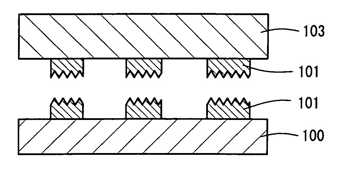
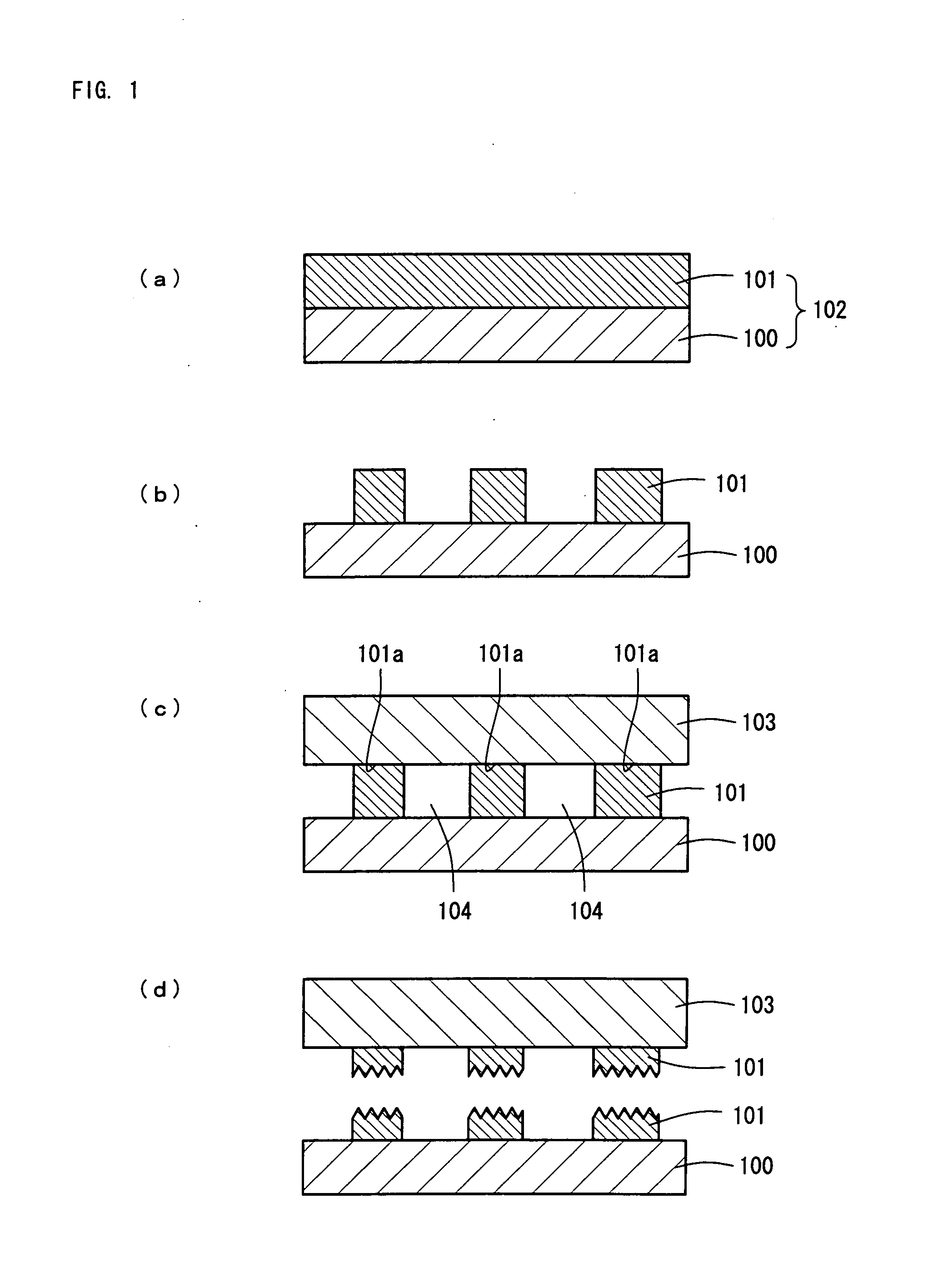
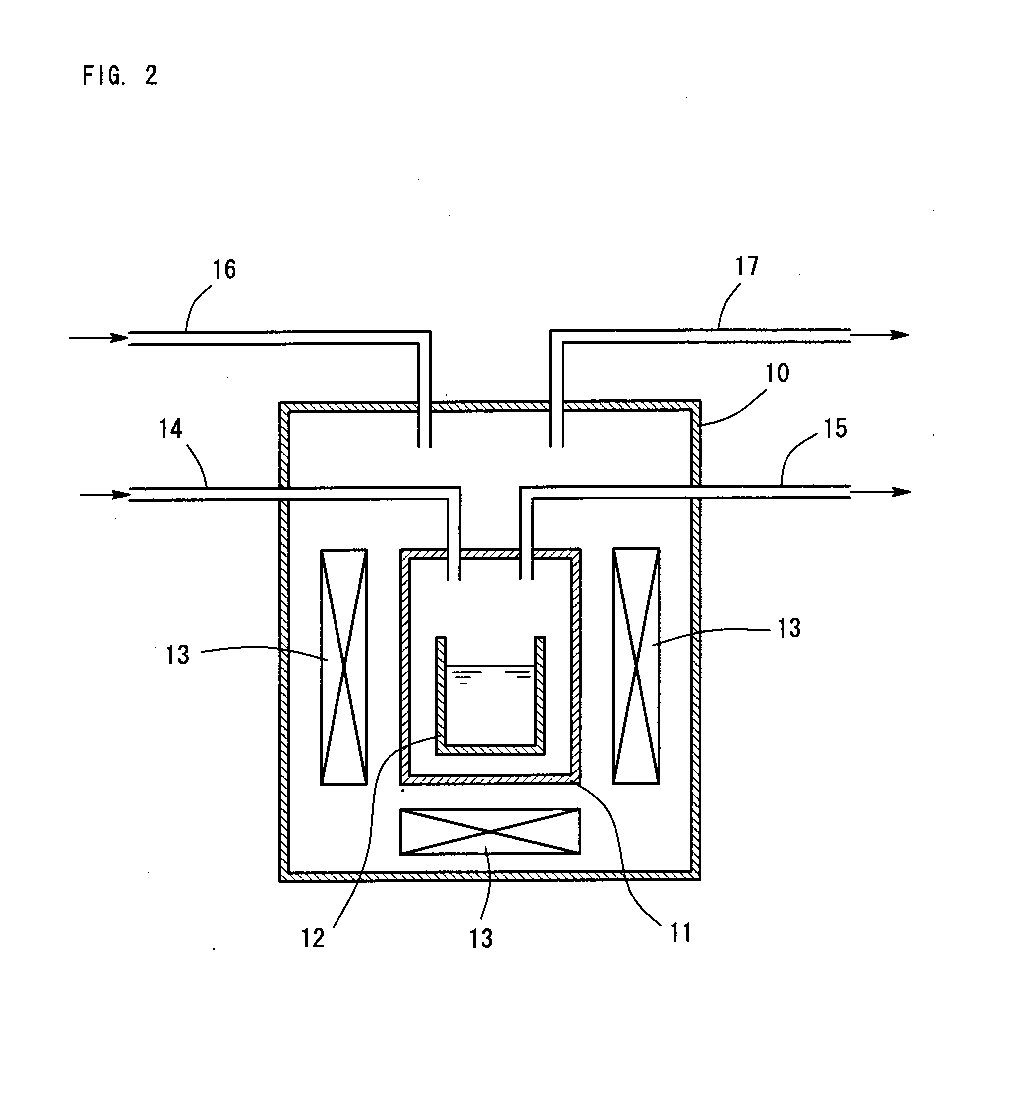
[0038]FIGS. 1A to 1D show the steps of producing a GaN crystal by the Na flux method performed in Embodiment 1. FIG. 2 shows an apparatus for producing the GaN crystal.

[0039]The configuration of the production apparatus will next be described. The production apparatus comprises a pressure container 10, a reaction vessel 11, a crucible 12, a heating apparatus 13, supply pipes 14, 16, and discharge pipes 15, 17.

[0040]The pressure container 10 is a pressure-resistant hollow cylinder made of stainless steel. To the pressure container 10, the supply pipe 16 and the discharge pipe 17 are connected. In the pressure container 10, the reaction vessel 11 and the heating apparatus 13 are disposed. The reaction vessel 11 has heat resistance. In the reaction vessel 11, the crucible 12 is placed. The crucible 12 holds a molten mixture containing Ga and Na, and a template substrate 102 is maintained in the molten mixture. To the reaction vessel 11, the supply pipe 14 and the discharge pipe 15 are ...

embodiment 2

[0051]The embodiment 2 is related with a template substrate 102 used in the method of the present invention for producing a Group III nitride semiconductor. FIGS. 3A and 3B show the steps of preparing the template substrate 102. An AlN buffer layer 201 was uniformly formed on a sapphire substrate 200. Subsequently a GaN layer 202 with a thickness of 2 μm was uniformly formed on the AlN buffer layer 201. A photoresist was uniformly formed on the GaN layer 202. Subsequently a periodic pattern mask of the photoresist was formed on the surface of the GaN layer 202 by a photolithography. Next a maskless portion was dry etched until the sapphire substrate 200 was exposed as shown in FIG. 3A. After removing the mask and cleaning the substrate, a GaN layer 203 was grown again by HVPE or MOVPE as shown in FIG. 3B. In this way, the template substrate 102 was formed. The template substrate which is formed by such a process can be used as the template substrate 102 of the embodiment 1.

[0052]The...


PUM

PropertyMeasurementUnit
thicknessaaaaaaaaaa
thicknessaaaaaaaaaa
pressureaaaaaaaaaa

Abstract

In the Na flux method, a target semiconductor layer is separated from a sapphire substrate of a template substrate. The template substrate formed of the sapphire substrate and a GaN layer is placed in a Ga—Na molten mixture. The temperature the molten mixture and the nitrogen pressure are adjusted to 850° C. and 2.5 MPa, respectively. Under the conditions, a part of the GaN layer is melted back until the surface of the sapphire substrate is exposed, so that the remaining portion of the GaN layer is left in the form of a plurality of upright columns. Then, the pressure is elevated to 3 MPa, whereby a target GaN layer is grown on the processed GaN layer. Through lowering temperature, stress due to the difference in linear expansion coefficient and lattice constant between sapphire and GaN is generated, to thereby generate cracks in the processed GaN layer. By virtue of the cracking, the target GaN layer is separated from the sapphire substrate.

Description

BACKGROUND OF THE INVENTION[0001]1. Field of the Invention[0002]The present invention relates to a method for producing a Group III nitride semiconductor by the flux method. More particularly, the invention relates to a method of separating a Group III nitride semiconductor layer from a sapphire substrate while cracking of the Group III nitride semiconductor layer grown by the flux method is prevented, in the case where a template substrate formed of the sapphire substrate and the Group III nitride semiconductor layer is employed as a seed crystal.[0003]2. Background Art[0004]The Na flux method is a known method for producing a Group III nitride semiconductor such as GaN. In this method, a molten mixture of Na (sodium) and Ga (gallium) is reacted with nitrogen at about 800° C. and a pressure of some ten atmospheres, to thereby grow GaN crystals.[0005]The Na flux method employs, as a seed crystal, for example, a template substrate formed of a sapphire substrate and a GaN layer grown ...

Claims


Application Information

Patent Timeline
Patent Type & Authority Applications(United States)
IPC IPC(8): C30B19/10C30B19/04
CPCC30B9/10C30B19/02C30B9/06C30B29/406C30B19/04C30B29/403
Inventor YAMAZAKI, SHIRO
Owner TOYODA GOSEI CO LTD
Why Eureka
Try Eureka