Semiconductor laser pumped solid-state laser device

a solid-state laser and semiconductor technology, applied in lasers, laser cooling arrangements, laser details, etc., can solve the problems of reducing the laser output that should be extracted as a light to the outside of the microchip, stable laser oscillation at high-power operation, and reducing the refractive index, so as to achieve stably generated, efficiently and stably emitted, and suppressed the effect of parametric oscillation in the microchip

Active Publication Date: 2011-07-21
INTER UNIV RES INST NAT INST OF NATURAL SCI
View PDF2 Cites 2 Cited by
  • Summary
  • Abstract
  • Description
  • Claims
  • Application Information

AI Technical Summary

Benefits of technology

[0032]According to the present invention, in the semiconductor laser pumped solid-state laser device, the parasitic oscillation in the microchip can be suppressed and the laser beam can be efficiently and stably emitted to the outside. In addition, the high-power and short-pulsed light can be stably generated.

Problems solved by technology

It is known, however, that since the energy difference between a pumping wavelength of the semiconductor laser and an oscillation wavelength of the solid-state laser turns into heat in the solid-state laser medium, the temperature increase due to the heat causes a change of a refractive index in the solid-state laser medium, as well as distortion or deformation resulting from thermal expansion, which prevents the stable laser oscillation at high-power operation.
When the parasitic oscillation occurs within the microchip, pumping energy absorbed in the core circulates around within the microchip as a parasitic oscillation light and turns into heat by being consumed within the microchip, resulting in the substantial decrease in laser output that should to be extracted as a light to the outside of the microchip.

Method used


Image

  • Semiconductor laser pumped solid-state laser device
  • Semiconductor laser pumped solid-state laser device
  • Semiconductor laser pumped solid-state laser device

Examples


embodiments

[0048]Hereinafter, the embodiments of the present invention will be described in detail.

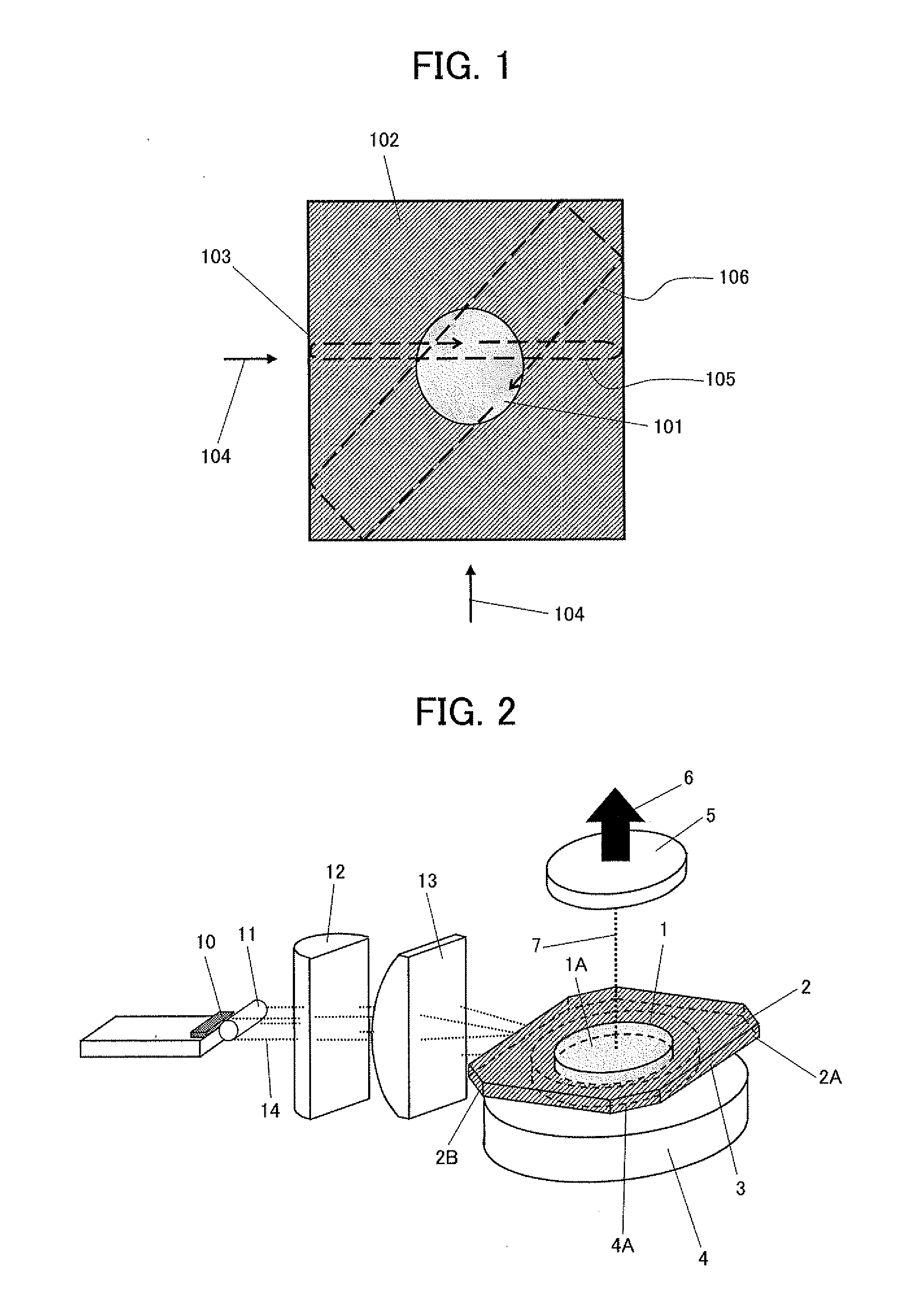
[0049]FIG. 2 shows a configuration of a semiconductor laser pumped solid-state laser device according to a first embodiment of the present invention.

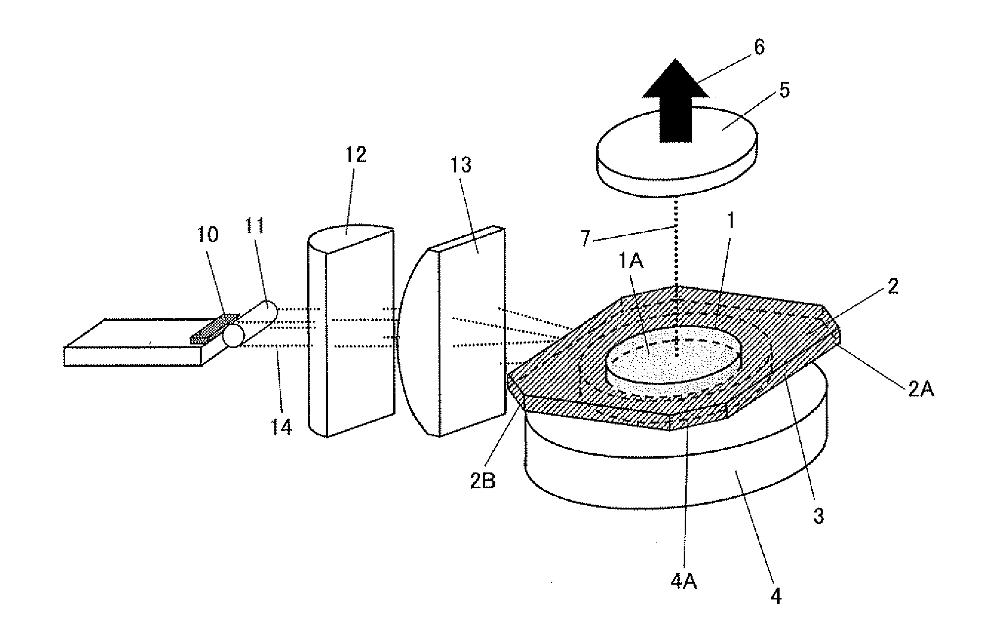
[0050]In this figure, a solid-state laser core 1 is circular-shaped with 2 mm in diameter, formed of a solid-state laser medium (Nd:YAG) containing YAG (yttrium aluminum garnet) as a base material of a microchip and 1 at % of Nd (neodymium) as a laser oscillation element, and fixedly mounted on an upper highly heat conductive section 4A of a heat sink 4 formed of CuW (copper tungsten). On its periphery, a light guide region 2 formed of the same base material, YAG, containing 5 at % of Sm (samarium) is formed, having four linear optical pumping windows 3 formed on an outer peripheral face 2A. Here, in order to allow efficient exhaustion of heat generated in the solid-state laser core 1, it is desirable for the solid-state laser core 1 and the light gu...


PUM


Abstract

A compact semiconductor laser pumped solid-state laser device is provided that can suppress unnecessary parasitic oscillation in a microchip and efficiently extract energy. The semiconductor laser pumped solid-state laser device comprises: a solid-state laser core 1 disposed in the center and formed of a laser medium containing neodymium (Nd) as a laser oscillation element; a light guide region 2 integrally formed around the solid-state laser core 1, having approximately rectangular shape with four linear light entrance windows formed on the outer periphery thereof, and containing samarium (Sm) as a laser oscillation element; and a heat sink 4 disposed on one face of the light guide region 2 including the solid-state core 1, wherein laser oscillation is performed by introducing a pumping light 14 through the light entrance windows 3 and propagating the pumping light 14 through the light guide region 2 to pump the solid-state laser core 1, and wherein a laser oscillation light is extracted from the upper face of the solid-state laser core 1 opposite to the face contacting the heat sink 4.

Description

BACKGROUND OF THE INVENTION[0001]1. Field of the Invention[0002]The present invention relates to a small-sized, high-power, highly efficient, and highly stable microchip solid-state laser device, and particularly to a semiconductor laser pumped solid-state laser device.[0003]2. Description of the Related Art[0004]Conventionally, a semiconductor laser pumped solid-state laser device can absorb optical energy from a plurality of semiconductor lasers into a solid-state laser medium, followed by converting the energy to a highly focusing laser beam having a uniform electromagnetic wavefront in a solid-state laser resonator. Thus, the very high optical density can be obtained by focusing the laser beam using lenses. As such, this type of laser device has been applied to a variety of common devices and systems, such as measuring light sources for physics and chemistry, as well as processing, e.g., cutting and welding, of various industrial materials.[0005]It is known, however, that since ...

Claims


Application Information

Patent Timeline
Patent Type & Authority Applications(United States)
IPC IPC(8): H01S3/04
CPCH01S3/042H01S3/1611H01S3/0941H01S3/06
Inventor TSUNEKANE, MASAKITAIRA, TAKUNORI
Owner INTER UNIV RES INST NAT INST OF NATURAL SCI
Why Eureka
Try Eureka