

Creep-resistant polishing pad window
a polishing pad and scratch-resistant technology, applied in the field of polymer windows, can solve the problems of increasing the cost of cmp consumables, and increasing the cost of manufacturing
- Summary
- Abstract
- Description
- Claims
- Application Information
AI Technical Summary
Benefits of technology
Problems solved by technology
Method used
Image

Examples
example 1
Comparative Window A
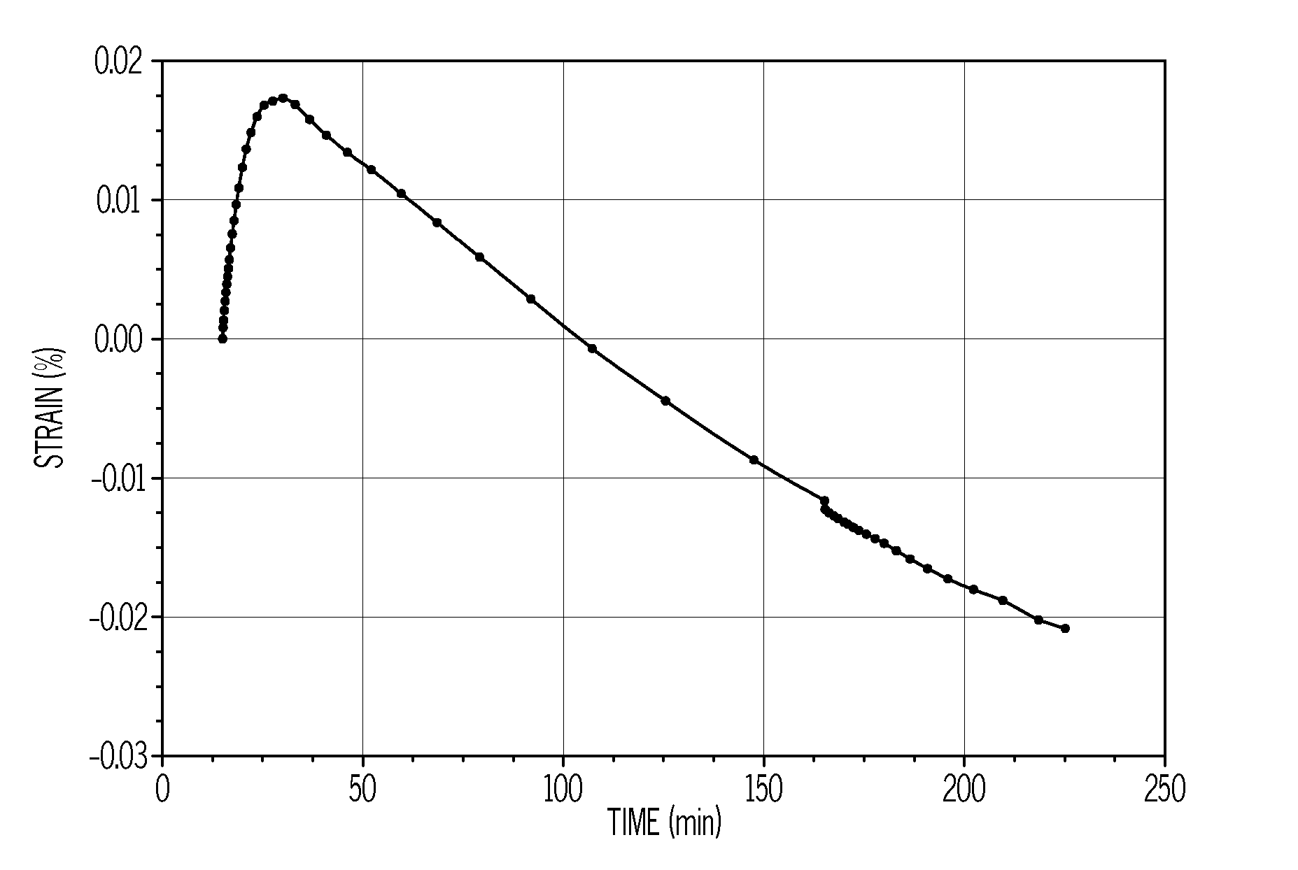
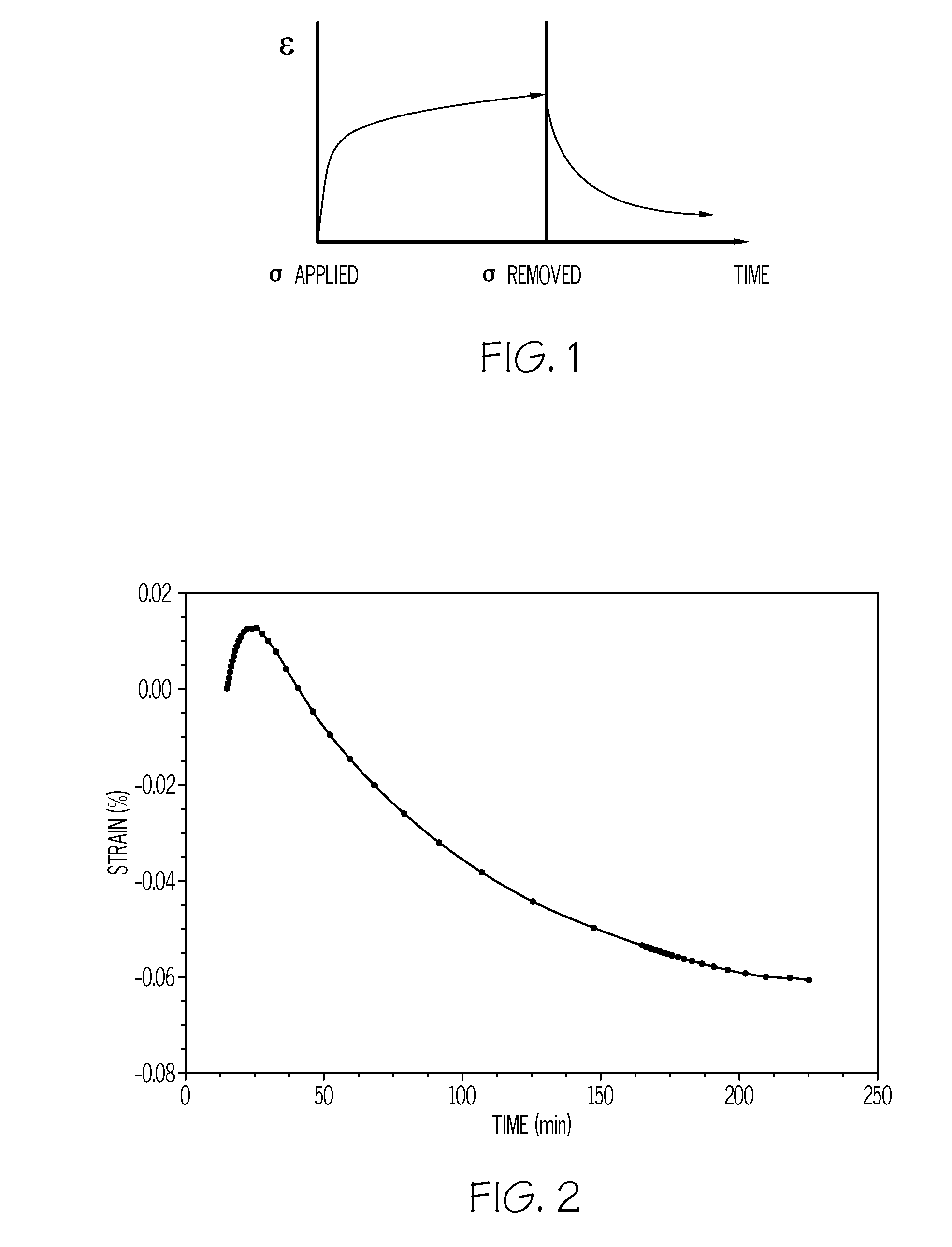
[0039]Comparative Window A was a commercially available window designed for use with an optical end point detection device that did not require transmission below 500 nm. The cross-linked polymer consisted of a prepolymer mixture containing aromatic and aliphatic isocyanate and an aromatic chain extender. The negative time dependent creep response of the as-manufactured sample is shown in FIG. 2. Instead of a continuous stretching of the sample with time as shown schematically in FIG. 1, the time dependent strain response of Window A shows a retraction of the sample along the extension direction as evidenced by the negative strain values. This retraction demonstrated a metastable polyurethane that retracted with time and temperature. The time dependent strain response of an annealed sample of Comparative Window A is shown in FIG. 3. After annealing the sample, the time dependent strain response resembled the time dependent strain shown schematically in FIG. 1. Ba...
example 2
Comparative Window B
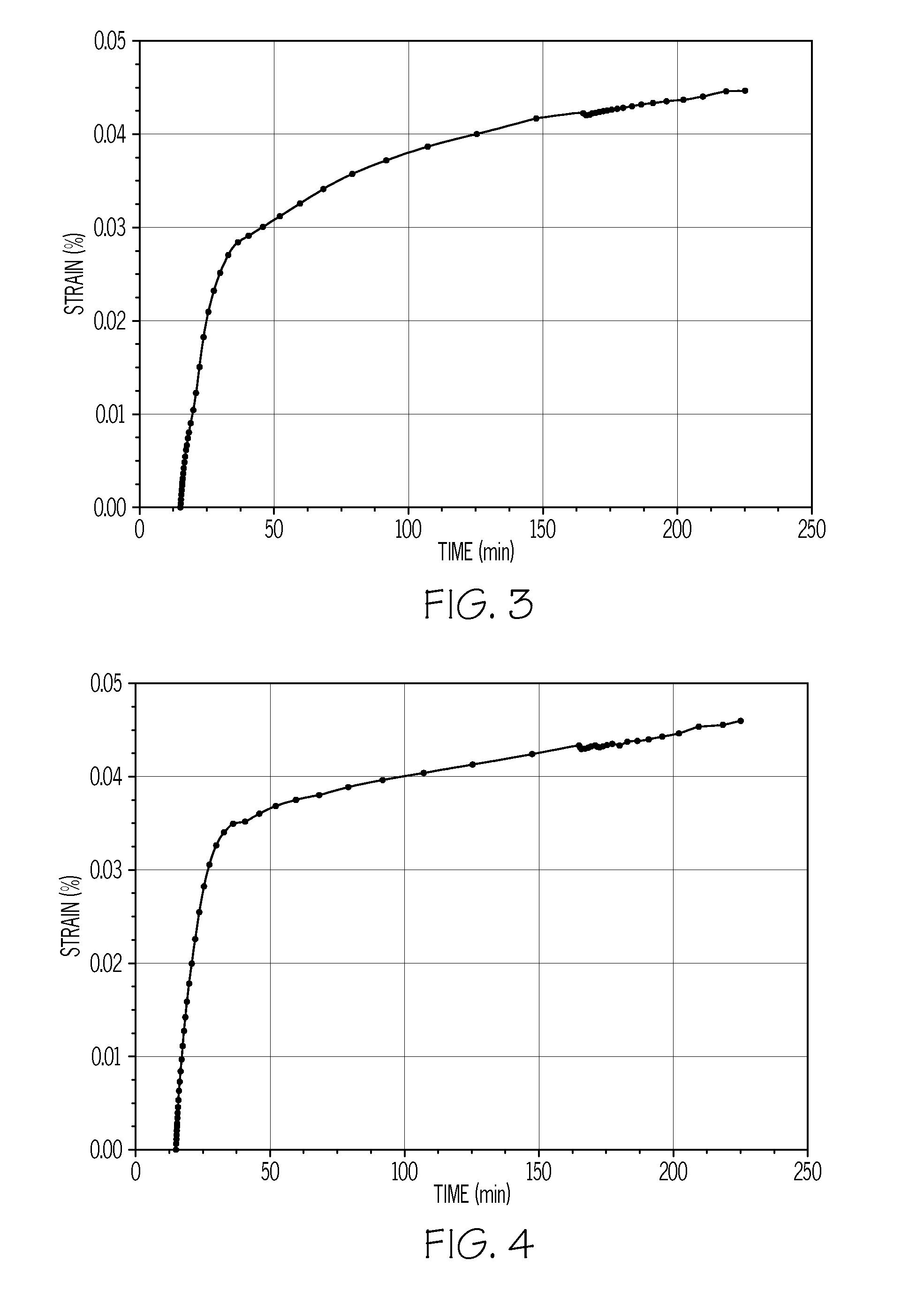
[0040]Comparative Window B represented an experimental material designed for use with an optical end point detection device that required significant transmission below 500 mn. The polymer consisted of an aliphatic prepolymer and an aromatic chain extender. Despite having a stoichiometry of 95%, the polymer exhibited very low cross-linking as evidenced by the swell test results. It is possible that inadvertent exposure to atmospheric moisture increased the stoichiometry, thereby decreasing both the degree of cross-linking and the molecular weight. At completion of the swell test, the sample was dissolved within the solution. Therefore, the final dimensions could not be measured and the results were not applicable. The lack of cross-linking also resulted in a larger time dependent strain than Comparative Window A as illustrated in FIGS. 4, 5, and Table 2. Annealing the sample reduced the metastable state to show a further increase in time dependent strain. Compara...
example 3
Comparative Window C
[0041]Comparative Window C was a commercially available window designed for use with optical end point detection devices that required significant transmission below 500 nm. The cross-linked polymer consisted of an aliphatic prepolymer and an aromatic chain extender. Comparative Window B and Comparative Window C were manufactured from different prepolymers. Referring to FIGS. 6, 7, and Table 2, the time dependent strain did not provide sufficient creep resistance for demanding window applications in either the as-manufactured or annealed state. Although the material maintained its integrity in the linear swell test better than did Comparative Window B, it would not be expected to have the chemical cross-linking of Comparative Window A because it was prepared at greater than one hundred percent stoichiometry. As illustrated by the linear swell results, chain entanglements, sometimes termed “physical cross-links”, may have contributed to the reduced time dependent ...
PUM
 Abstract
Description
Claims
Application Information