Thin film transistor and display device

a technology of thin film transistor and display device, which is applied in the direction of semiconductor devices, basic electric elements, electrical appliances, etc., to achieve the effect of reducing the time to be taken for film formation, stabilizing electrical characteristics, and suppressing oxygen desorption

Active Publication Date: 2011-07-28
JOLED INC
View PDF2 Cites 88 Cited by
  • Summary
  • Abstract
  • Description
  • Claims
  • Application Information

AI Technical Summary

Benefits of technology

[0011]The invention is proposed in consideration of such problems, and a first object thereof is to provide a thin film transistor that is capable of suppressing desorption of oxygen and others from an oxide semiconductor layer, and reducing the time to be taken for film formation, and to provide a display device provided therewith.
[0012]A second object of the invention is to provide a thin film transistor that is capable of suppressing reduction of oxygen in an oxide semiconductor that is caused by hydrogen in the air, and suppressing desorption of oxygen and others from an oxide semiconductor layer, and to provide a display device provided therewith.
[0017]In the first thin film transistor in the embodiment of the invention, a laminated film is provided on the side of the gate electrode of the oxide semiconductor layer, and on the side opposite to the gate electrode. The laminated film includes the first layer made of aluminum oxide, and the second later made of an insulation material including silicon (Si). Accordingly, in the resulting configuration, the oxide semiconductor layer is sandwiched on both sides by the first layer made of aluminum oxide. This thus suppresses the desorption of oxygen and others from the oxide semiconductor layer, thereby stabilizing the electrical characteristics. Moreover, since the second layer is made of an insulation material including silicon (Si), the time to be taken for film formation can be reduced compared with a previous gate insulation layer configured by a single layer of aluminum oxide.
[0019]According to the first thin film transistor in the embodiment of the invention, on the side of the gate electrode of the oxide semiconductor layer, and on the side opposite to the gate electrode, provided is the laminated film including the first layer made of aluminum oxide, and the second later made of an insulation material including silicon (Si). Accordingly, in the resulting configuration, the oxide semiconductor layer can be sandwiched on both sides by the first layer made of aluminum oxide. This thus suppresses the desorption of oxygen and others from the oxide semiconductor layer, thereby stabilizing the electrical characteristics. Moreover, since the second layer is made of an insulation material including silicon (Si), the time to be taken for film formation can be reduced compared with a previous gate insulation layer configured by a single layer of aluminum oxide.
[0020]In the second thin film transistor in the embodiment of the invention, the passivation film is made of an oxide, nitride, or oxynitride containing one or more of aluminum (Al), titanium (Ti), and tantalum (Ta). Such a configuration can suppress the reduction of oxygen in the oxide semiconductor layer that is caused by the hydrogen in the air, and also can suppress the desorption of oxygen and others in the oxide semiconductor layer.

Problems solved by technology

However, such a previous passivation film is not yet considered enough in view of protection, and there thus has been a demand for the development of a passivation film having the enhanced capabilities of being able to serve as a barrier against the oxygen and hydrogen.

Method used


Image

  • Thin film transistor and display device
  • Thin film transistor and display device
  • Thin film transistor and display device

Examples


first embodiment

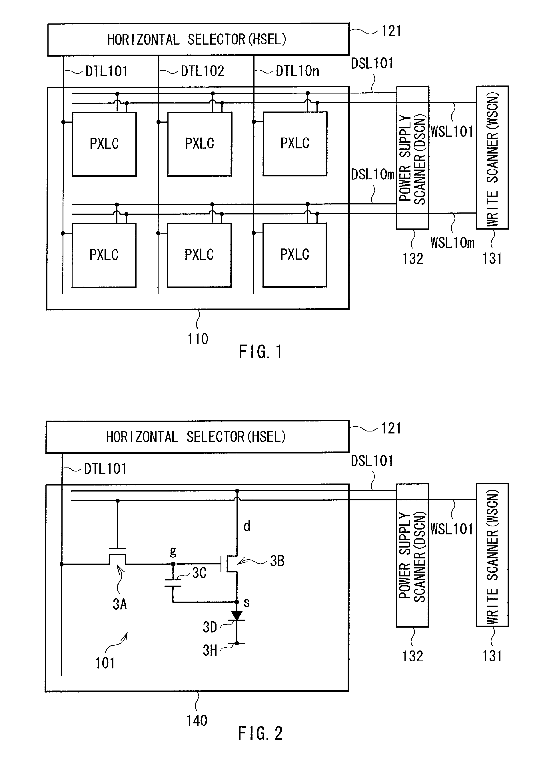
[0048]FIG. 1 is a diagram showing the configuration of a display device in a first embodiment of the invention. This display device is for use as an ultra-thin organic light-emitting color display device. For example, in this display device, a TFT substrate 1 that will be described later is provided thereon with a display region 110, in which pixels PXLC are arranged in a matrix. The pixels PXLC are each configured by any one of a plurality of organic light-emitting elements 10R, 10G, and 10B each being a display element and will be described later. This display region 110 is provided therearound with a horizontal selector (HSEL) 121 being a signal section, a write scanner (WSCN) 131 and a power supply scanner (DSCN) 132 each being a scanner section.

[0049]In the display region 110, signal lines DTL 101 to 10n are arranged in a column direction, and in a row direction, scan lines WSL 101 to 10m and power supply lines DSL 101 to 10m are arranged. At each intersection between the signa...

modified example 1

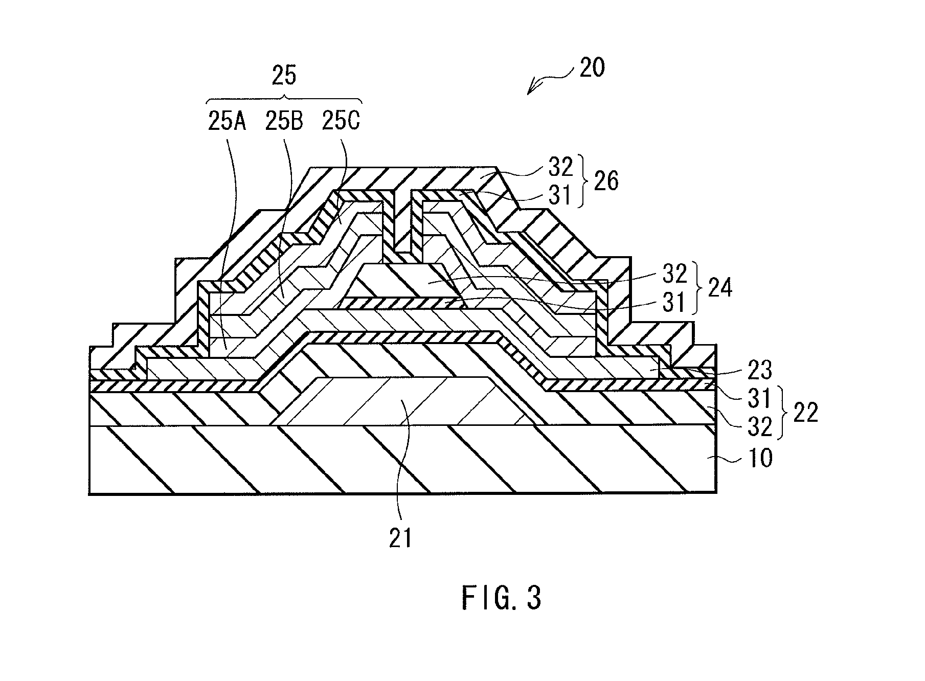
[0092]Note that, in the first embodiment described above, exemplified is the case in which the gate insulation film 22, the channel protection layer 24, and the passivation film 26 each have the laminate configuration including the first layer 31 made of aluminum oxide, and the second layer 32 made of an insulation material including silicon (Si). Alternatively, as shown in FIG. 7, only the gate insulation film 22 and the channel protection layer 24 may each have the laminate configuration including the first layer 31 made of aluminum oxide, and the second layer 32 made of an insulation material including silicon (Si). This configuration also enables to reduce the influence of gas such as oxygen by sandwiching the oxide semiconductor layer 23 between the first layer 31 of the gate insulation film 22 and the first layer 31 of the channel protection layer 24, thereby being able to increase the stability and reliability of the electrical characteristics of the TFT 20.

[0093]In this case...

modified example 2

[0094]Still alternatively, as shown in FIG. 8, only the gate insulation film 22 and the passivation film 26 may each have the laminate configuration including the first layer 31 made of aluminum oxide and the second layer 32 made of an insulation material including silicon (Si). This configuration also enables to reduce the influence of gas such as oxygen by sandwiching the oxide semiconductor layer 23 between the first layer 31 of the gate insulation film 22 and the first layer 31 of the passivation film 26, thereby being able to increase the stability and reliability of the electrical characteristics of the TFT 20.

[0095]In this case, the channel protection layer 24 has the thickness of about 300 nm, for example, and is configured by one or more of an aluminum oxide film, a silicon oxide film, a silicon nitride film, and a silicon oxynitride film.


PUM


Abstract

Provided are a thin film transistor that is capable of suppressing desorption of oxygen and others from an oxide semiconductor layer, and reducing the time to be taken for film formation, and a display device provided therewith. A gate insulation film 22, a channel protection layer 24, and a passivation film 26 are each in the laminate configuration including a first layer 31 made of aluminum oxide, and a second layer 32 made of an insulation material including silicon (Si). The first and second layers 31 and 32 are disposed one on the other so that the first layer 31 comes on the side of an oxide semiconductor layer 23. The oxide semiconductor layer 23 is sandwiched on both sides by the first layers 31 made of aluminum oxide, thereby suppressing desorption of oxygen and others, and stabilizing the electrical characteristics of a TFT 20. Moreover, since the second layer 32 is made of an insulation material including silicon (Si), the time to be taken for film formation can be reduced compared with a single layer made of aluminum oxide.

Description

TECHNICAL FIELD[0001]The present invention relates to a thin film transistor (TFT) including an oxide semiconductor layer as a channel, and a display device provided therewith.[0002]2. Background Art[0003]An oxide semiconductor such as zinc oxide or indium gallium zinc oxide (IGZO) has the excellent characteristics to serve as an active layer of a semiconductor device, and recently is under development with the aim of application to a TFT, a light-emitting device, a transparent conductive film, and others.[0004]For example, a TFT using an oxide semiconductor is with a high electron mobility and with excellent electrical characteristics compared with the one in which a channel is amorphous silicon (a-Si: H) previously used in a liquid crystal display device. Such a TFT also has advantages of possibly achieving a high mobility even at a low temperature of about room temperature.[0005]On the other hand, the oxide semiconductor is known to be not heat resistant enough, and to cause latt...

Claims


Application Information

Patent Timeline
Patent Type & Authority Applications(United States)
IPC IPC(8): H01L33/00H01L29/04
CPCH01L27/1225H01L27/3211H01L29/7869H01L27/3262H01L27/3244H10K59/35H10K59/1213H10K59/12H01L29/4908H01L29/78606
Inventor MOROSAWA, NARIHIROTERAI, YASUHIROARAI, TOSHIAKI
Owner JOLED INC
Why Eureka
Try Eureka