Solid-state imaging apparatus, method of manufacturing same, and electronic apparatus

a technology of solid-state imaging and manufacturing methods, applied in the direction of electrical apparatus, semiconductor devices, transistors, etc., can solve the problems of increased difficult control, and achieve the effects of improving image characteristics, reducing variations in overflow barriers, and reducing the influence of mask misalignmen

Active Publication Date: 2011-07-28
SONY SEMICON SOLUTIONS CORP
View PDF10 Cites 15 Cited by
  • Summary
  • Abstract
  • Description
  • Claims
  • Application Information

AI Technical Summary

Benefits of technology

[0026]According to the solid-state imaging apparatus in accordance with an embodiment of the present invention, it is possible to suppress variations in an overflow barrier in a horizontal overflow structure so as to improve pixel characteristics.
[0027]According to the method of manufacturing a solid-state imaging apparatus in accordance with an embodiment of the present invention, an overflow barrier of a horizontal overflow structure can be formed without be...

Problems solved by technology

It is understood that since the dosage of the n-type impurity to be ion-implanted below the transfer gate electrode has...

Method used


Image

  • Solid-state imaging apparatus, method of manufacturing same, and electronic apparatus
  • Solid-state imaging apparatus, method of manufacturing same, and electronic apparatus
  • Solid-state imaging apparatus, method of manufacturing same, and electronic apparatus

Examples


first embodiment (

2. First embodiment (example of configuration of solid-state imaging apparatus and example of manufacturing solid-state imaging apparatus)

second embodiment (

3. Second embodiment (example of configuration of solid-state imaging apparatus and example of manufacturing solid-state imaging apparatus)

third embodiment (

4. Third embodiment (example of configuration of electronic apparatus)

1. Example of Overall Configuration of CMOS Solid-State Imaging Apparatus

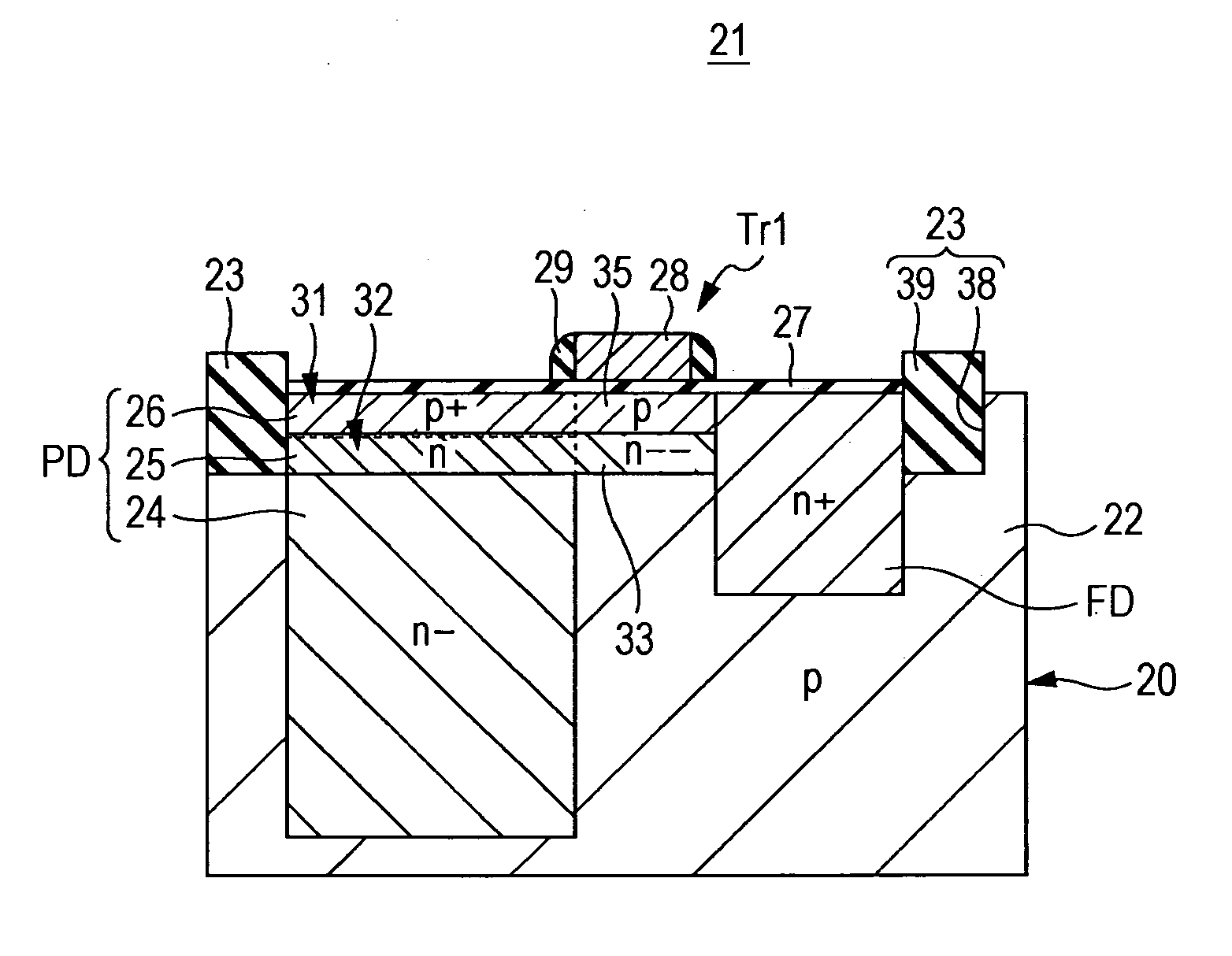
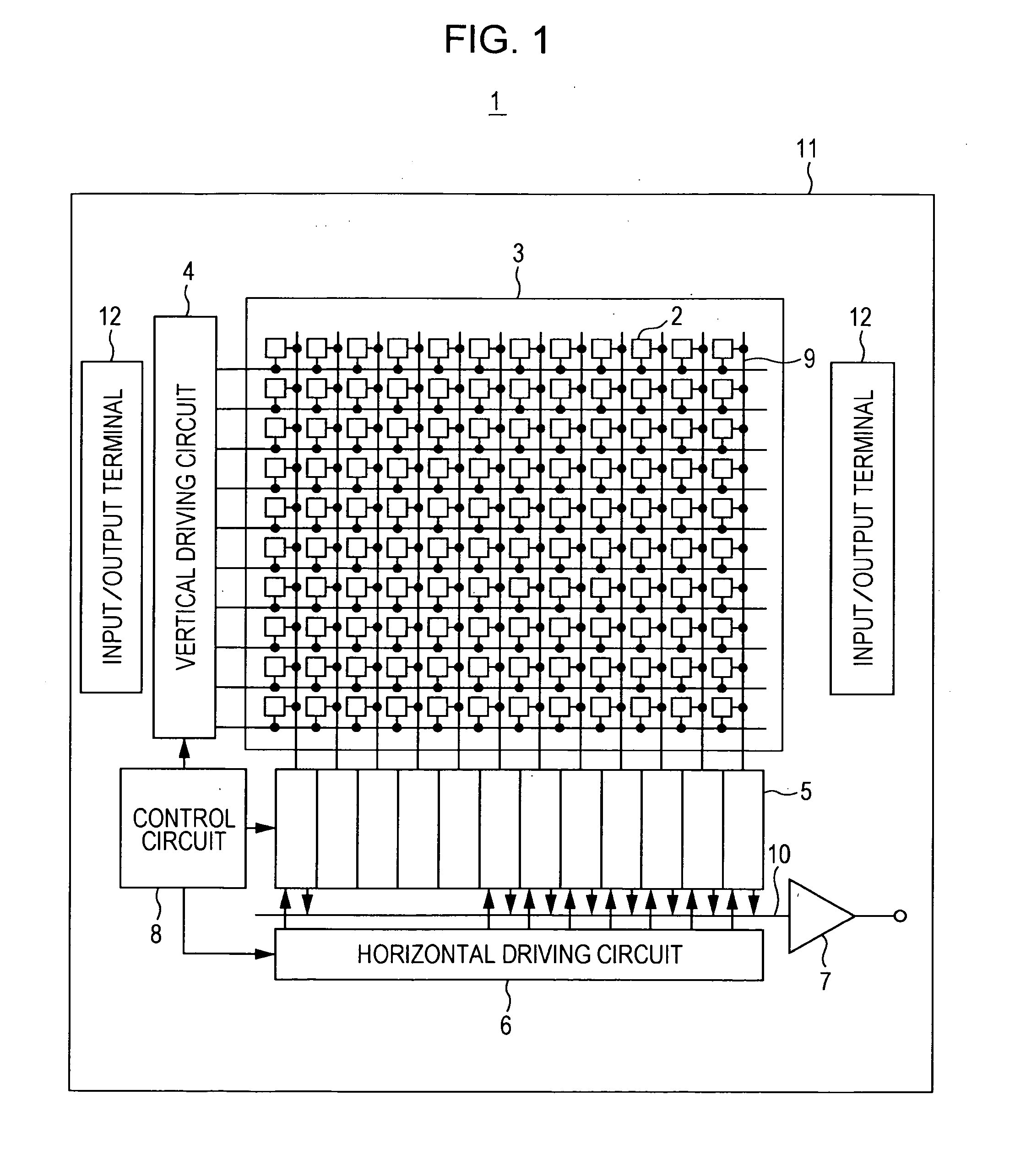
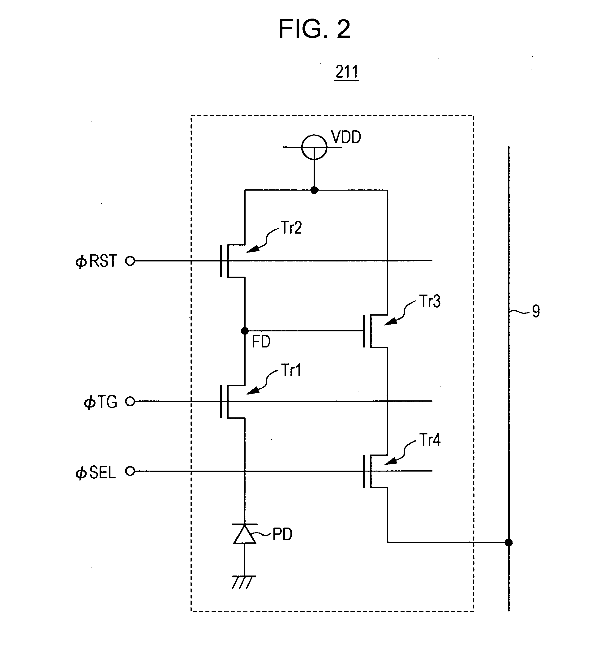
[0044]FIG. 1 shows an overall configuration of an example of a MOS solid-state imaging apparatus according to each of the embodiments of the present invention. As shown in FIG. 1, a solid-state imaging apparatus 1 of this example is configured to include a pixel area (so-called image-sensing area) 3 in which a plurality of pixels 2 including a photoelectric conversion unit are two-dimensionally arranged in a regular manner on a semiconductor substrate 11, for example, a silicon substrate, and a peripheral circuit unit. As the pixel 2, a unit pixel made up of one photoelectric conversion unit and a plurality of pixel transistors can be used. Furthermore, as the pixel 2, a so-called pixel shared structure in which a plurality of photoelectric conversion units share other pixel transistors excluding the transfer transistor can be used. The plura...


PUM


Abstract

A solid-state imaging apparatus includes a plurality of pixels each including a photoelectric conversion unit and pixel transistors, which are formed on a semiconductor substrate; a floating diffusion unit in the pixel; a first-conductivity-type ion implantation area for surface pinning, which is formed over the surface on the side of the photoelectric conversion unit and the surface of the semiconductor substrate; and a second-conductivity-type ion implantation area for forming an overflow path serving as an overflow path for the floating diffusion unit, the second-conductivity-type ion implantation area being formed below the entire area of the first-conductivity-type ion implantation area. An overflow barrier is formed using the second-conductivity-type ion implantation area. A charge storage area is formed using an area in which the second-conductivity-type semiconductor area and the second-conductivity-type ion implantation area superpose each other.

Description

BACKGROUND OF THE INVENTION[0001]1. Field of the Invention[0002]The present invention relates to a solid-state imaging apparatus, a method of manufacturing the solid-state imaging apparatus, and an electronic apparatus used for, for example, a camera including the solid-state imaging apparatus.[0003]2. Description of the Related Art[0004]An example of a solid-state imaging apparatus is a CMOS solid-state imaging apparatus. Because CMOS solid-state imaging apparatuses have a low power-supply voltage and have low consumption of power, they are used for digital still cameras, digital video cameras, various portable terminal devices such as mobile phones with camera, printers, and the like.[0005]CMOS solid-state imaging apparatuses are configured to include a pixel area in which a plurality of pixels constituted by a photodiode that is a photoelectric conversion unit and a plurality of pixel transistors are two-dimensionally arranged in a regular manner, and a peripheral circuit unit ar...

Claims


Application Information

Patent Timeline
IPC IPC(8): H01L31/113H01L31/18
CPCH01L27/1461H01L27/14616H01L27/14689H01L27/14641H01L27/1463
Inventor YAMADA, AKIHIROYAMAMOTO, ATSUHIKOKIDO, HIDEO
Owner SONY SEMICON SOLUTIONS CORP
Why Eureka
Try Eureka