Piezoelectric film element, and manufacturing method of the same and piezoelectric film device

a piezoelectric film and manufacturing method technology, applied in the direction of piezoelectric/electrostrictive device material selection, piezoelectric/electrostrictive/magnetostrictive device material selection, device material selection, etc., can solve the problems of poor piezoelectric film element production yield, high piezoelectric constant, and difficult to obtain piezoelectric film device having high reliability, etc., to achieve the effect of improving piezoelectric properties, ensuring the quality pi

Active Publication Date: 2011-08-04
SUMITOMO CHEM CO LTD
View PDF13 Cites 24 Cited by
  • Summary
  • Abstract
  • Description
  • Claims
  • Application Information

AI Technical Summary

Problems solved by technology

However, in a piezoelectric material manufactured by a manufacturing method typified by a sintering method, being a method performed conventionally, as its thickness becomes thinner, particularly as the thickness becomes closer to the thickness of about 10 μm, this thickness becomes closer to the size of a crystal grain constituting the material, and its influence can not be ignored.
However, in a conventional technique, it is difficult to obtain the piezoelectric film element having high piezoelectric properties uniformly, and a production yield of the piezoelectric film element is poor, and also it is difficult to obtain the piezoelectric film device having high reliability.
As a result, when an actuator or a sensor is manufactured by using the Si substrate, it is difficult to stably produce a lead-free device having a long service-life and a high piezoelectric constant.

Method used


Image

  • Piezoelectric film element, and manufacturing method of the same and piezoelectric film device
  • Piezoelectric film element, and manufacturing method of the same and piezoelectric film device
  • Piezoelectric film element, and manufacturing method of the same and piezoelectric film device

Examples


an embodiment

[0054]A structure of a piezoelectric film element according to an embodiment of the present invention, a manufacturing method of a lower electrode using a sputtering method, and a lattice strain analysis method of the lower electrode will be described hereafter.

(Structure of the Piezoelectric Film Element)

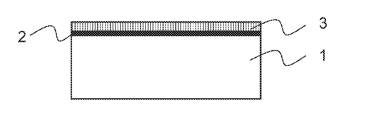
[0055]As shown in FIG. 5, the piezoelectric film element of this embodiment has a substrate 1; an oxide film (not shown) formed on a surface of the substrate 1; a lower electrode 3 formed on the oxide film; and a perovskite type piezoelectric film 6 formed on the lower electrode 3. The piezoelectric film 6 is expressed by (NaxKyLiz)NbO3(0≦x≦1, 0≦y≦1, 0≦z≦0.2, x+y+z=1), with the lower electrode 3 oriented in a prescribed direction, and the piezoelectric film 6 preferentially oriented in the prescribed direction with respect to the lower electrode 3.

[0056]As the substrate 1, Si substrate, MgO substrate, ZnO substrate, SrTiO3 substrate, SrRuO3 substrate, a glass substrate, a quartz gl...

example 1

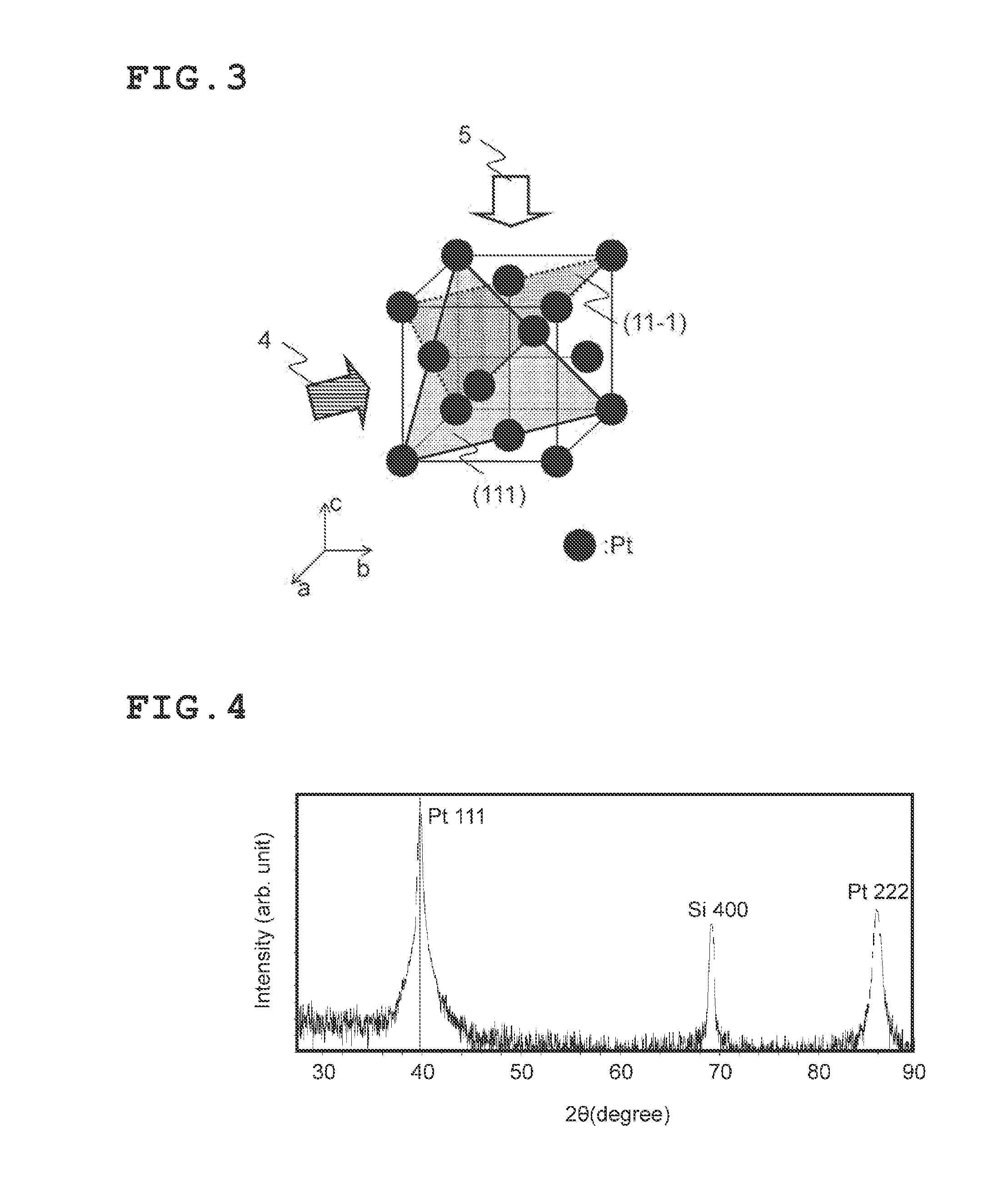
[0092]In example 1, the Pt lower electrode film with (111) preferential orientation was formed on the substrate with an oxide film, to thereby manufacture the substrate with the Pt film, and further the KNN film with (001) preferential orientation was formed on the Pt lower electrode film, to thereby manufacture the substrate with the piezoelectric film.

(Formation of the Substrate with the Pt Film)

[0093]FIG. 1 shows a schematic cross-sectional structure of the substrate with the Pt film according to the example 1. The substrate with the Pt film is formed, so that SiO2 film (not shown), Ti bonding layer 2, and Pt lower electrode 3 are sequentially formed on the Si substrate 1.

[0094]Next, the manufacturing method of the substrate with the Pt film according to the example 1 will be described.

[0095]First, thermal oxide film SiO2 (film thickness 100 nm) was formed on the surface of the Si substrate 1 ((100) plane direction, thickenss: 0.5 mm, size: 20 mm×20 mm). Next, Ti bonding layer 2 ...

example 2

Pt Electrode Strain Analysis

[0102]In example 2, a lattice strain analysis of the Pt lower electrode manufactured in the example 1 was performed.

[0103]In the lattice strain analysis of the Pt electrode according to the example 2, X-ray diffractometer with high power rotating anode was used, having a two-dimensional detector mounted thereon, and having an X-ray detection area of a large area.

[0104]When a large-sized substrate of 4 inches and 6 inches was used, as the lattice strain analysis of the Pt electrode, the lattice strain was evaluated by using the X-ray diffractometer with high power rotating anode having a two-dimensional detector mounted thereon, and having an X-ray detection area of a large area (a solid angle of a wide range), by cutting the large-sized substrate into 20 mm square so that a sample can be accommodated in an analyzer. Note that in a device provided with a sample stage for a substrate having a large area, the lattice strain analysis can be performed in a sta...


PUM


Abstract

A piezoelectric film element is provided, which is capable of improving piezoelectric properties, having on a substrate at least a lower electrode, a lead-free piezoelectric film, and an upper electrode, wherein at least the lower electrode out of the lower electrode and the upper electrode has a crystal structure of a cubic crystal system, a tetragonal crystal system, an orthorhombic crystal system, a hexagonal crystal system, a monoclinic crystal system, a triclinic crystal system, a trigonal crystal system, or has a composition in which one of these crystals exists or two or more of them coexist, and crystal axes of the crystal structure are preferentially oriented to a specific axis smaller than or equal to two axes of these crystals, and a ratio c / a′ is set in a range of 0.992 or more and 0.999 or less, which is the ratio of a crystal lattice spacing c in a direction of a normal line to the substrate surface, with respect to a crystal lattice spacing a′ whose inclination angle from the substrate surface is in a range of 10° or more and 30° or less.

Description

FIELD OF THE INVENTION[0001]The present invention relates to a piezoelectric film element using lithium potassium sodium niobate and a manufacturing method of the same, and a piezoelectric film device.DESCRIPTION OF THE RELATED ART[0002]A piezoelectric ceramics is processed into various piezoelectric elements according to various purposes, and is widely used as an actuator for generating deformation by applied voltage, and a functional electronic component such as a sensor for generating the voltage from the deformation of the piezoelectric element. A lead-based dielectric material having high piezoelectric properties is generally known as the piezoelectric ceramics utilized for the purpose of usage in the actuator and the sensor. Particularly, Pb (Zr1-xTix) O3-based perovskite ferroelectric material called PZT has been generally known heretofore. Ordinarily, these piezoelectric materials are formed by sintering an oxide made of a piezoelectric material.[0003]Meanwhile, in recent ye...

Claims


Application Information

Patent Timeline
Patent Type & Authority Applications(United States)
IPC IPC(8): H01L41/047H01L41/09H01L41/18H01L41/187H01L41/22H01L41/29H01L41/316H01L41/319H02N2/00
CPCH01L41/047H01L41/1873H01L41/187H10N30/877H10N30/1051H10N30/2042H10N30/8542H10N30/06H10N30/076H10N30/853
Inventor SUENAGA, KAZUFUMISHIBATA, KENJIWATANABE, KAZUTOSHINOMOTO, AKIRA
Owner SUMITOMO CHEM CO LTD
Why Eureka
Try Eureka